
Chapter 1 Fundamentals of Quantitative Design and Analysis
1.1 Computer Architecture
Computer architecture includes instruction set architecture, organization/microarchitecture (high-level aspects), hardware/system design (hardware components). The following are the seven dimensions of instruction set architecture:
Categories of ISA
| Stack | Accumulator | Register (register-memory) | Register (load-store) |
|---|---|---|---|
| Push A | Load A | Load R1, A | Load R1, A |
| Push B | Add B | Add R1, B | Load R2, B |
| Add | Add R3, R1, R2 | ||
| Pop C | Store C | Store C, R1 | Store C, R3 |
Memory Address - All ISAs are byte-addressable
addressing mode
RISC-V (base model)
- Register
- Immediate
- Displacement (base + offset)
x86 / 80x86 (extends RISC-V style addressing)
- No register (absolute addressing)
- Two registers (base + index)
- Scaled index (base + index × constant)
ARMv8 (extends RISC-V)
- PC-relative addressing
Operand Types and Sizes - Integers come in 8-bit, 16-bit, 32-bit, and 64-bit, while floating-point numbers are available in 32-bit and 64-bit. The 80x86 also supports 80-bit.
Operations - Data transfer, arithmetic logic, control, floating-point numbers
Control flow instructions - Including conditional branches, unconditional jumps, procedure calls, and returns, all using PC-relative addressing
Condition Checking
- RISC-V → compare registers directly
- x86 / ARMv8 → use condition codes (flags)
Return Address Storage
- RISC-V → register (ra)
- ARMv8 → register (LR)
- x86 → stack (memory)
ISA Encoding - Both ARMv8 and RISC-V have fixed-length instructions of 32 bits; 80x86 instructions are variable-length, ranging from 1 to 18 bytes.
1.2 Quantitative Principles of Computer Design
Leverage parallelism: data parallelism / instruction-level parallelism / data-level parallelism
Principle of locality: temporal locality / spatial locality
Focus on the common case
Amdahl’s Law: The performance improvement gained by using a faster mode of execution is limited by the fraction of time the faster mode can be used.
CPU-related formulas can be found in the computer organization notes.
Chapter 2 Memory Hierarchy Design
Latency: Determines the time it takes to retrieve the first data word in a data block
Bandwidth: Determines the time it takes to access the remaining content in the data block
2.1 Memory Hierarchy
Memory Technologies
SRAM
- Static storage, no need for refresh, fast speed, but high cost and high power consumption
- Mainly used to build high-speed cache
DRAM
- Dynamic storage, requires periodic refresh, low cost, high density
- DRAM is organized into multiple banks, each containing rows and columns
- Performance optimization
- Synchronous DRAM (SDRAM): Supports burst transfer, allowing continuous transmission of multiple data after a row activation
- DDR (double data rate) SDRAM: Transmits data on both the rising and falling edges of the clock
- Multi-bank parallel access: Allows simultaneous access to data in different banks, further increasing bandwidth.
Flash Memory
- Non-volatile, data is not lost after power-off
- NOR flash has fast random read and write speeds, but slow write speeds and high cost; NAND flash has high density, low cost, suitable for large-capacity storage, but slower read and write speeds
- Random access latency is much higher than DRAM, but it has high density and low cost
Phase-Change Memory (PCM)
- Stores data by changing the resistance state of the material
Techniques for Higher Bandwidth
Wider Main Memory: Increasing the width of cache and memory
- Disadvantages: Requires the use of MUX that increases latency on critical paths; complicates error correction
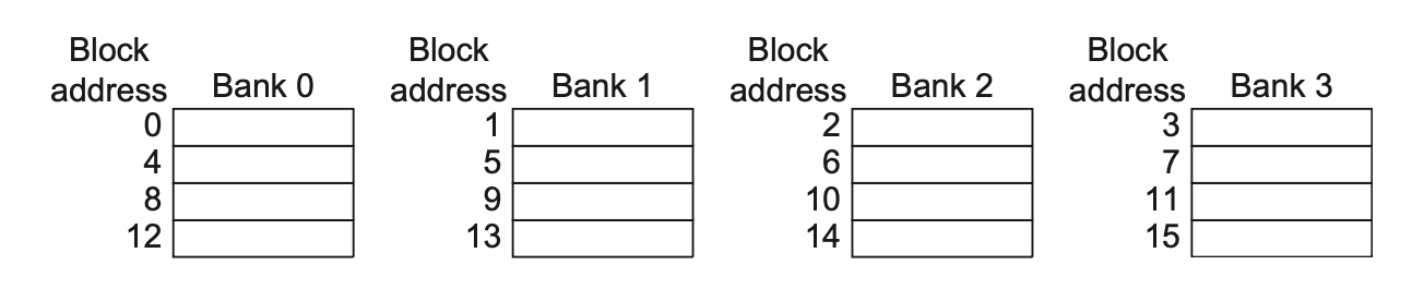
Simple Interleaved Memory: Organizing memory into multiple partitions, allowing simultaneous reading and writing of multiple words.
- Achieves multi-way interleaved access by sharing address lines and data buses
- Leverages parallelism across multiple chips in the memory system
- Regarding partition access
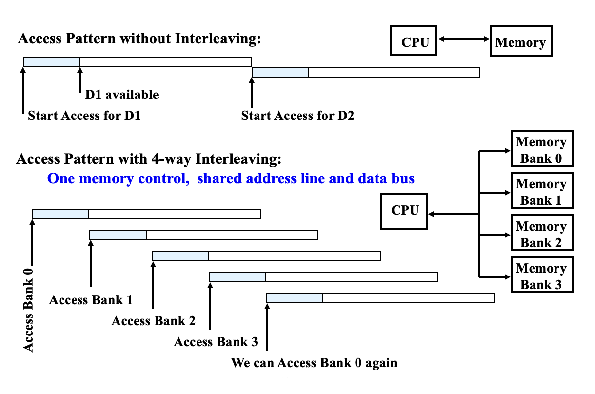
Independent Memory Partitions: Provide independent memory controllers, address lines, and data buses for each partition.
- The number of partitions should be greater than the number of clock cycles required to access a word in a partition to avoid waiting.
- Partition conflicts occur when array size or access patterns cause multiple elements to map to the same memory partition, leading to CPU stalls. Solutions include:
- Loop interchange: Change the order of nested loops to avoid accessing the same partition.
- Expand array size: Make it not a power of two to force address mapping to different partitions.
- Use a prime number of memory partitions.
Four Memory Hierarchy Questions
Block Placement
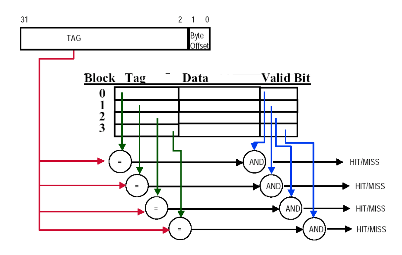
Direct mapped: Each data block has only one specific location in memory.
Fully associative: Data blocks can be placed anywhere in memory.
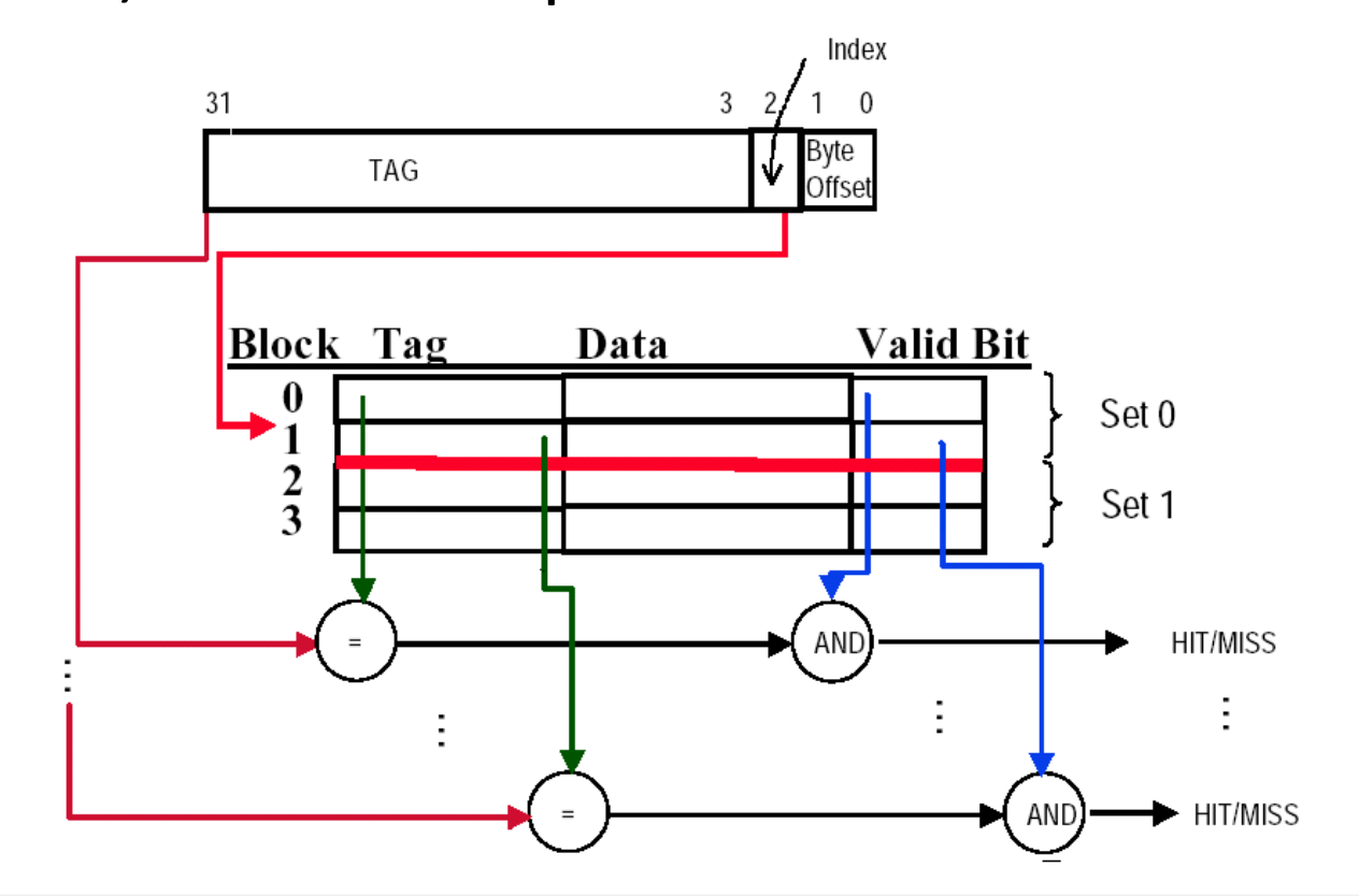
N-way set associative: Each data block is restricted to a specific set in memory and can be placed in any of the n locations within that set.
Direct mapped = 1-way set associative, Fully associative = N-way set associative
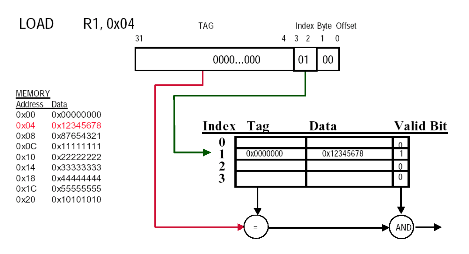
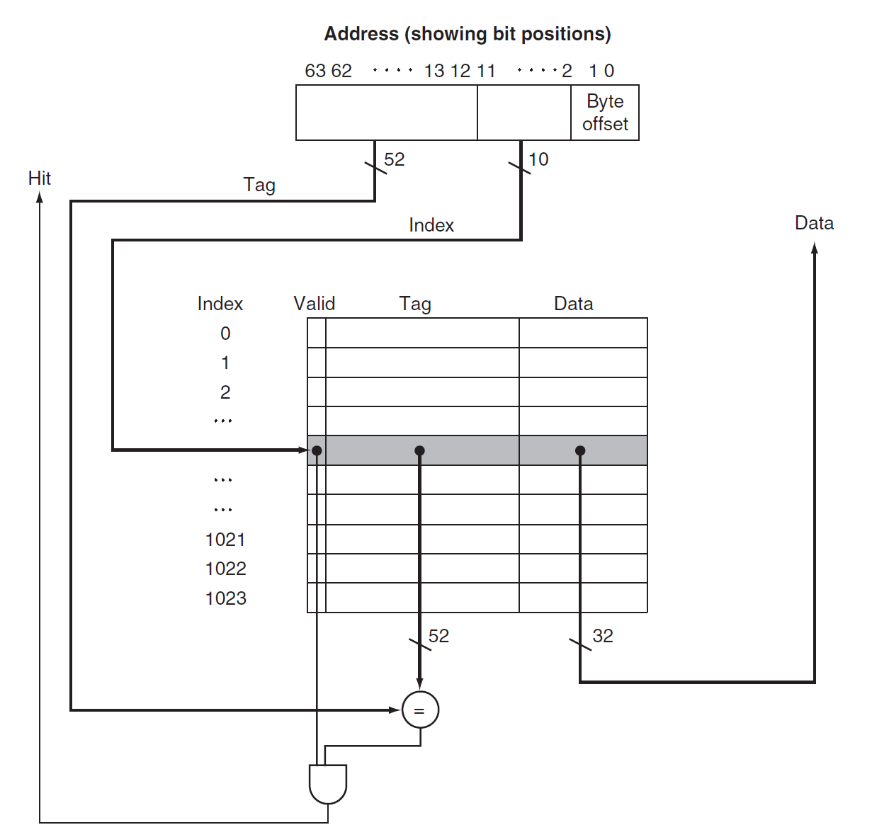
Block Identification
The unique address of each cache block is divided into multiple fields as follows:
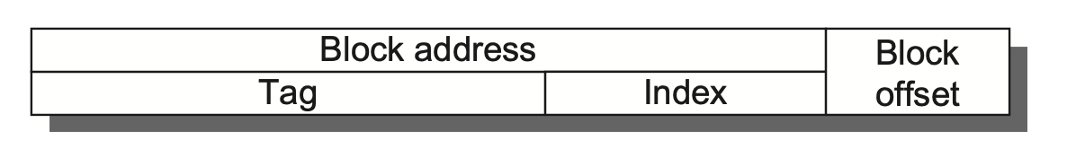
block address:
- tag
- index: In set-associative mapping, used to select a specific set, number of bits =
block offset: number of bits =
valid bit: If this bit is 0, it indicates that the address is invalid
Block Replacement
When a failure occurs, the controller must decide which data block to replace in order to store the data required by the processor.
For direct mapping: No selection is needed; a specific data block is directly replaced.
For set-associative and fully associative:
- Random: Randomly selects a block, which is simple to implement but may evict recently accessed blocks.
- Least Recently Used (LRU): Replaces the data block that has not been used for the longest time, with the drawback of being complex to implement.
- First In, First Out: Replaces the oldest existing data block, which is an approximate implementation of LRU.
Write Strategy
Two Strategies for Write Hits
Write through: Information is written to both the data block in the cache and the data block in the next level of memory, with the advantage of being simple to implement.
- Write stall: The processor must wait for the write-through to complete before proceeding to the next step. An optimization method is to add a write buffer, allowing the processor to continue executing subsequent tasks while data is being written into the buffer.
Write back: Information is only written into the data block of the cache. Once a modified data block (dirty block) in the cache is about to be replaced, this data block must be written to the next level of memory to ensure that previous updates are applied to the underlying memory.
- Introduce a dirty bit as a status bit to record the modification status of a data block.
Two Strategies for Write Misses
- Write allocate: Load the entire data block containing the target address from main memory (or the next level of cache) into the cache (corresponding to Write back)
- No-write allocate/Write around: Write directly to main memory (corresponding to Write through)
2.2 Cache
unified cache: Instructions and data share the same cache space
split cache: Instructions and data have their own independent cache spaces
Performance
The number of memory stall cycles is jointly determined by the number of misses and the miss penalty.
Failure loss and failure rate may differ in read and write scenarios, so they can be discussed separately if necessary.
average memory access time, AMAT:
例子还没看,实在看不进去,好让人没有食欲的题目、、、
Impact of Caches on Processor Performance
For an in-order processor, AMAT can indeed predict the processor’s performance; however, for an out-of-order processor (which will be introduced in later chapters), it is not that simple.
The lower the CPI of execution, the greater the relative impact of the number of cache miss cycles.
Even for two computers with the same memory hierarchy, a processor with a higher clock frequency will have more clock cycles per miss, so the proportion of memory in the CPI will be higher.
Out-of-Order Execution Processors
Define “failure loss”:
We need to consider the length of memory latency and the length of latency overlap.
When evaluating the trade-offs of memory hierarchy, designers typically use simulators for out-of-order processors and memory to verify that measures aimed at improving average memory latency indeed enhance program performance.
Basic Optimizations
Three directions to improve cache performance:
- Reduce miss rate
- Reduce miss penalty
- Reduce hit time
Classification of miss situations:
- Compulsory: A miss inevitably occurs when accessing a data block in the cache for the first time, as the corresponding data block must first be brought into the cache.
- Capacity: The cache cannot contain all the required data blocks.
- Conflict: For set-associative or direct-mapped caches, multiple data blocks map to the same set, causing earlier stored data to be replaced.
Summary of Six Basic Cache Optimization Methods:
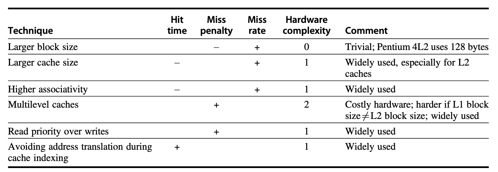
+indicates a positive effect on the factor,-indicates a negative effect on the factor, and a blank indicates no effect
Larger Block Size
Leveraging the advantage of spatial locality reduces the occurrence of forced conflicts.
Increasing the penalty of misses, as the number of data blocks decreases, leading to conflict misses and even capacity misses.
The selection of data block size needs to consider both the latency and bandwidth of the lower-level memory. If both latency and bandwidth are high, consider using larger data blocks; otherwise, use smaller ones.
Larger Caches
It may result in longer hit times, as well as higher costs and power consumption.
Higher Associativity
Two rules of thumb:
- The effect of reducing misses with an 8-way set-associative cache is nearly equivalent to that of a fully associative cache.
- For a direct-mapped cache of size N, its miss rate is equal to that of a 2-way set-associative cache of size N/2.
The trade-off is an increase in hit time, so increasing the degree of associativity is not recommended for processors with high clock frequencies.
Multilevel Caches
First, consider the simplest scenario—a two-level cache hierarchy:
- L1 can be made small enough to keep up with the processor’s clock cycles, affecting the processor’s clock frequency.
- L2 can be made large enough to capture more memory accesses, with its speed only impacting the penalty of L1 misses.
The formula for AMAT becomes:
Local miss rate: Number of misses in a specific cache / Total number of memory accesses to that cache
Global miss rate (better for multilevel cache): Number of misses in a specific cache / Total number of memory accesses from the processor
The number of misses per instruction can be used as a metric, calculated as:
The associativity of L2 also affects the overall cache miss penalty.
Multilevel Inclusion: Data from L1 will always appear in L2,
- This ensures data consistency.
- The drawback is that additional processing is required for multilevel caches with different block sizes.
Multilevel Exclusion: Data from L1 will never appear in L2,
- This is suitable when L2 is only slightly larger than L1.
- When a miss occurs in L1, data is swapped between L1 and L2.
Giving Priority to Read Misses over Writes
In the write-through strategy, we utilize the write buffer to enhance its performance.
The write buffer may contain the latest updated value for a certain location, and the data at this location may be requested during a read miss.
If a read operation directly fetches data from main memory while the data in the write buffer has not yet been written to main memory, it can lead to a RAW data hazard (i.e., reading stale data).
The optimization method is: when a read miss occurs, check the contents of the write buffer.
If the address of the read request exists in the write buffer (meaning there is pending latest data to be written), fetch the data directly from the write buffer.
If there is no conflict and the memory system is available, allow the read miss to proceed and fetch data from main memory.
Regarding write-back caches:
When a read miss requires replacing a “dirty” memory block, copy the dirty block to the write buffer.
Then immediately read the new block from main memory.
The write-back operation of the dirty block is handled in the background by the write buffer.
The processor also needs to check the write buffer for conflicting addresses during a read miss.
Avoiding Address Translation During Indexing of the Cache
For indexes and tags, virtual addresses are not used entirely (i.e., VIVT (Virtual Index, Virtual Tag))
Although it can eliminate the time required for translation
Considering the page-level protection mechanism when converting virtual addresses to physical addresses
- Solution: Copy the protection information on the TLB when it becomes invalid, store this information in a field, and check it each time the virtual cache is accessed
Ambiguity problem: Whenever a process is switched, the same virtual address points to a different physical address, requiring a cache flush operation
- Solution: Increase the width of the address tag bits to serve as a process-identifier tag (PID)
The operating system and user programs may use two different virtual addresses to refer to the same physical address
Solution 1: Antialiasing, ensuring that each cache data block corresponds to a unique physical address
Solution 2: Force these aliases to share some address bits, a restriction known as page coloring
Virtual Index, Physical Tag (VIPT): A method that leverages the advantages of both virtual and physical caches simultaneously.
Uses the portion of the virtual and physical addresses where the page offset is identical to index the cache.
While using this index to read the cache, translates the virtual portion of the address.
And matches the tag with the physical address.
This approach enables immediate reading of cache data while still using the physical address for comparison.
Advanced Optimizations
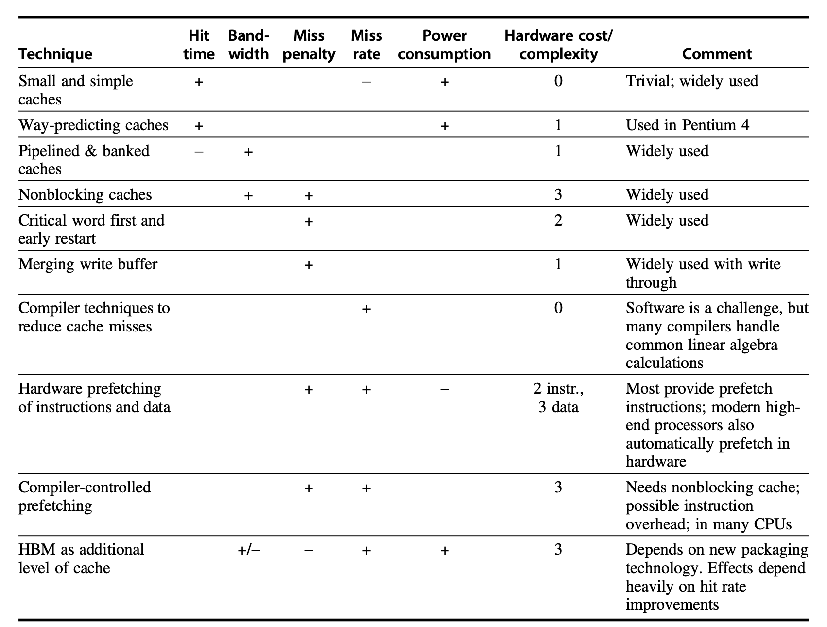
Small and Simple First-Level Caches
Reduce the size of the first-level cache, or lower its associativity
Way Prediction
Keep extra bits in the cache (called block predictor bits) to predict the next data block that may be accessed.
If the prediction is correct: The cache access latency is the fast hit time.
If the prediction fails: Try the next data block, change the predictor’s content, and incur an additional clock cycle delay.
A major drawback of this method is that it increases the difficulty of pipelining cache accesses.
Pipelined Access and Multibanked Caches
These optimization methods primarily target L1.
The approach of multiple partitions can also be applied to L2 and L3 caches, but it is mainly used as a power management technique.
Pipelined Access: Results in a higher number of clock cycles at the cost of increased latency.
Multibanked Caches: The cache is divided into independent partitions, each supporting independent access.
How addresses are mapped to partitions affects the behavior of the memory system.
Sequential interleaving: A mapping method that evenly distributes addresses to each partition in order.
Nonblocking Caches
Non-blocking caches allow data to continue providing hits even when cache misses occur, leveraging the potential advantages of out-of-order pipeline CPUs.
A method to further reduce the penalty of cache misses is “hit under multiple miss” or “miss under miss,” which involves overlapping multiple misses.
The characteristic that cache misses do not cause the processor to stall increases the difficulty of evaluating the performance of non-blocking caches. The effective miss penalty is the non-overlapping time that causes the processor to stall. The benefits of non-blocking caches depend on the penalties from multiple misses, memory reference patterns, and the number of instructions the processor can execute while outstanding misses are pending.
Out-of-order processors can hide the penalty of L1 misses that hit in L2 but cannot hide the penalties from lower-level cache misses.
Implementing a non-blocking high-speed cache is challenging for the following reasons:
Arbitration for contention between hits and misses
- Solution: Give higher priority to hits, then order conflicting misses
Tracking outstanding misses to determine when to allow load and store operations to proceed
- Solution: Use a miss status handling register (MSHR) to record outstanding misses and their associated information.
Critical Word First and Early Start
critical word first: Request the invalid word data from memory, and once the data is obtained, immediately send it to the processor, allowing the processor to continue executing instructions while the remaining words in the data block are being filled.
early start: Once the required word data is obtained, send it to the processor and allow the processor to continue executing instructions.
It only provides significant benefits when the cache data block is large, but it is difficult to calculate the penalty of invalidation.
Merging Write Buffer
Write-back sometimes also uses a write buffer.
Write merging: If the address of new data matches a valid entry in the write buffer, the new data is merged into that entry.
If the write buffer is full and there is no address match, the cache (and processor) must wait until there is an empty entry in the write buffer.
This allows for more efficient use of memory and also reduces the number of stalls.
Compiler Optimizations
For instructions:
Reorder processes in memory to reduce conflict misses
Analyze whether instruction conflicts occur
For data:
Merging arrays: Represent composite elements with a single array to improve spatial locality
Loop interchange: Sometimes, by swapping the inner and outer loops, the order of data access better matches the order of data storage. This reduces miss rates by improving spatial locality
Loop fusion: Merge two independent loops that have the same iteration pattern and overlapping variables
Blocking: Divide a large array into smaller blocks (blocks), and solve the entire array by addressing each small block separately. This leverages both spatial and temporal locality. Example: Matrix multiplication
Hardware Prefetching of Instructions and Data
Core idea:
Use non-blocking cache to allow overlapping memory access during execution.
Prefetch instructions and data into the cache or external buffer in advance before the processor requests the data.
Instruction Prefetching: usually done by the hardware outside the cache
When the instruction fails, the processor will not only request the currently missing instruction block, but also pre-take the next consecutive instruction block.
These pre-retried blocks will be placed in the instruction stream buffer.
If the requested block is already in the stream buffer, cancel the original cache request and send the next pre-get request.
Data Prefetching: the above method is also applicable to data access
Disadvantages:
If the pre-pickup and the actual demand access compete for bandwidth, the performance may be reduced.
If the pre-acquired data is not used in the end, it will waste memory bandwidth and cache space.
Useless pre-tached data may expel the really useful data in the cache.
Pre-pickup operation will consume additional power consumption.
Compiler-Controlled Prefetching
Using a compiler, insert prefetch instructions for requested data before the processor fetches it.
Register prefetch: Loads a value into a register.
Cache prefetch: Loads data only into the cache.
Prefetch instructions that are not error-triggered will automatically become no-ops if they would normally cause an exception.
The most effective prefetching is “semantically invisible” to the program: prefetching does not alter the contents of registers or memory, and it does not cause virtual address errors. This type of prefetching is also known as nonbinding prefetch.
Loops can be used for prefetch optimization.
Issuing prefetch instructions incurs additional instruction overhead.
Using HBM to Extend the Memory Hierarchy
HBM: high bandwidth memory
Core Idea: Reduce the frequency of “opening new rows” and strive to accomplish more work within the same row.
Loh and Hill (L-H) Scheme:
Store tags and data in the same row of HBM SDRAM.
While opening a row is time-consuming, accessing different parts of the same row significantly reduces latency.
The L4 cache is organized as a 29-way set-associative structure, with each row containing a set of tags and 29 data segments.
Qureshi and Loh (Alloy Cache) Scheme:
An improvement upon the L-H scheme, integrating tags and data together.
Adopts a direct-mapped cache structure.
Reduces L4 access time to a single HBM cycle (through direct indexing and burst transfers).
Trade-off: Significantly reduces hit time but slightly increases miss rate.
Solutions for the problem of miss latency:
Use mapping to track the presence of blocks in the cache
Use a memory access predictor (based on historical prediction techniques) to predict possible misses. Small predictors can predict misses with high accuracy, thereby reducing the penalty of misses
2.3 Virtual Memory
Virtual memory divides physical memory into blocks and allocates them to different processes.
Shared and protected memory space
Automatic management of memory hierarchy
Simplifies the loading of executable programs
Reduces the time to start programs
Common Concepts in Virtual Memory
Page: A fixed-length block of virtual memory data, where a fixed-length address is divided into a page number and a page offset.
Segment: A variable-length block of virtual memory data, using one word to represent the segment number and another word to represent the segment offset.
Advantages and disadvantages of the two methods:
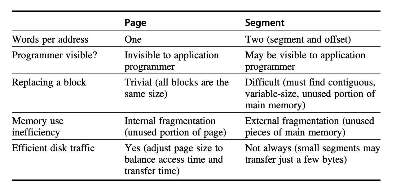
Page fault/address fault (analogous to cache miss)
Virtual address and physical address
Memory mapping/address translation
Four Memory Hierarchy Questions Revisited
Data Block Placement: Fully Associative
- Reason: The penalty for virtual memory misses is extremely high.
Data Block Identification: Indexed by page/segment number to locate the corresponding page/segment.
Typically, a data structure called the page table is used to store the physical addresses of virtual memory data blocks (for segments, offsets are also stored).
The size of the page table equals the number of pages in the virtual address space.
Inversed page table: A hash function is applied to the virtual address, making its size equal to the number of physical pages in memory.
- To reduce address translation time, a Translation Lookaside Buffer (TLB) is often used.
Data Block Replacement: LRU (Least Recently Used)
- A use/reference bit is employed. The operating system periodically clears the use bit and then sets it again, allowing it to track page access over a period of time.
Write Strategy: Write-Back
Reason: The significant difference in access times between memory and the processor.
The virtual memory system uses a dirty bit, allowing data blocks to be written to the hard disk when they are modified due to being read from the hard disk.
Techniques for Fast Address Translation
TLB: Leveraging the principle of locality, it retains translations for some addresses in a special cache.
The tag field stores the virtual address.
The data field stores the physical page number, protection fields, valid bit, and possibly usage and dirty bits.
If the physical page number or protection information in the page table is changed, the operating system must invalidate the corresponding entry in the TLB.
Operations within the TLB during address translation:
Send the virtual address to all tags.
Check the memory access type against the protection information in the TLB.
The matching tag sends the physical address to the MUX.
Concatenate the page offset with the physical page frame to form the final physical address.
Page Size
Reasons for using larger pages:
Save storage space for page tables
Utilize larger caches
Make full use of secondary storage
More memory can be effectively mapped, reducing TLB misses
Reasons for using smaller pages:
Conserve storage space
Speed up process startup
Adopting multiple page sizes: Achieve both benefits
Protection
Multiprogramming: Concurrently running programs share the resources of a single computer.
Process: Includes the program currently running and the state in which the program is running.
Time-sharing: A variant of multiprogramming that shares processor and memory resources among multiple interactive users, making it appear as if each user has their own computer.
Process/Context Switch: The act of switching from one process to another at any given time.
Since processes may be interrupted or switched multiple times, computer (hardware) and operating system designers are responsible for ensuring correct process behavior. Specifically:
Computer designers ensure that the processor-related state of a process can be saved and restored.
Operating system designers ensure that processes do not interfere with each other by partitioning memory to ensure that different processes have their own state at the same time.
Each process has its own page table, pointing to different memory pages, to protect the process.
Ring: A protection mechanism of the processor, divided into user, kernel, and possibly more privilege levels.
In addition to protection mechanisms, computers must also provide shared code and data between processes to allow inter-process communication or to save memory space by reducing copies of the same information.
2.4 The Design of Memory Hierarchies
Protection, Virtualization and Instruction Set Architecture
Virtual memory and virtualization technologies impose new demands on processor architecture and operating systems, necessitating adjustments to the instruction set architecture to support these functionalities.
Autonomous Instruction Fetch Units
Modern out-of-order execution and deep pipeline processors typically use independent instruction fetch units. These units can fetch entire instruction blocks and prefetch them into the L1 cache, thereby reducing instruction cache miss penalties. Although this may increase the miss rate of the data cache (because data that is not immediately needed is prefetched), the overall miss penalty is reduced.
Speculation and Memory Access
Speculation
Based on branch prediction, speculative execution is attempted before the processor determines whether the instruction truly needs to be executed.
If speculation is incorrect, speculative instructions in the pipeline are cleared, potentially causing unnecessary memory references, which can increase cache miss rates.
When combined with prefetching techniques, speculation can actually reduce the overall penalty of cache misses.
Special Instruction Caches
To meet the high instruction bandwidth demands of superscalar processors, a small cache can be used to store recently translated micro-operations, which helps reduce the penalty caused by branch prediction errors.
Coherency of Cached Data
When there are multiple copies of data, we need to ensure the consistency (coherency) of this data.
I/O cache coherency: When I/O devices interact with cached data, it is necessary to ensure that the data involved in I/O operations remains consistent with the data in the cache. Otherwise, it may cause the processor to see stale data or stall while waiting for I/O.
Solutions:
- Invalidate cache entries
- Flush buffers
Chapter 3 Instruction-Level Parallelism and Its Exploitation
3.1 Introduction
Instruction-level parallelism (ILP) allows instructions to be computed in parallel.
The CPI calculation formula for a pipelined CPU is: Pipeline CPI = Ideal pipeline CPI + Structural stalls + Data hazard stalls + Control stalls
Basic block: A small sequence of code that satisfies both that no branch enters it (unless it is the entry) and that no branch exits from it (unless it is the exit).
To achieve sufficient performance improvement, we should exploit ILP across multiple basic blocks.
Dependences in Instructions
When designing ILP, we must consider whether there are dependencies between instructions. Dependencies are generally divided into three types: data dependence, name dependence, and control dependence, which will be introduced in detail below.
Data Dependences
If instruction j data depends on instruction i through some path, then we say instruction j is data-dependent on instruction i.
If there is a data dependency between two instructions, the execution order of these two instructions must be preserved, and they must not be executed simultaneously.
A data dependency conveys three things, which are precisely the limitations it imposes on ILP:
The probability of a hazard occurring
The order in which results must be computed
The upper limit of parallelism that can be exploited
Of course, we certainly hope to overcome the above limitations—we can do so through two different approaches:
Maintain the dependency but avoid hazards. A common practice is to perform appropriate scheduling of the code, which can be implemented by the compiler or hardware.
Eliminate the dependency by modifying the code.
Name Dependences
When two instructions use the same register or memory location (referred to as a name), but there is no data flow between the two instructions regarding that name, a name dependence is considered to have occurred. There are two types of name dependences (assuming instruction j follows instruction i in program order):
Antidependence: Instruction j writes to a register or memory location that instruction i reads.
Output dependence: Both instruction i and instruction j write to the same register or memory location.
Such instructions can be executed in parallel or reordered, as long as the names (registers or memory locations) used by these instructions are changed to avoid conflicts.
For registers, this renaming operation is easier (referred to as register renaming) and can be handled by the compiler or dynamically by hardware.
Data Hazards
hazard: When there is a name or data dependency between instructions, if such instructions are close enough to be overlapped in execution, the order of accessing and depending on related operands may be altered, and a hazard occurs.
For data hazards, based on the read and write access order of instructions, they are classified into the following types (still assuming that instruction j comes after instruction i in program order):
RAW (read after write): j attempts to read a source operand before i writes to it, so j will obtain the old data. This is the most common type of hazard and corresponds to a true data dependency (i.e., true dependence).
// r1 has RAW
add r1, r2, r3
sub r4, r1, r3
WAW (Write After Write): j attempts to write to an operand before i has written to it, causing an incorrect execution order of write operations. The final result of the operand is the value written by i, not j. This hazard corresponds to an output dependency and only exists in pipelines that allow writing data in multiple stages, or in cases where instructions are allowed to continue executing while the preceding instruction is stalled.
// r1 has WAW
add r1, r2, r3
sub r1, r4, r3
WAR (Write After Read): j attempts to write to a destination operand before i reads it, causing i to incorrectly obtain the new data. This hazard corresponds to an anti-dependency and does not occur in most statically issued pipelines.
  // r1 has WAR
sub r4, r1, r3
add r1, r2, r3
Control Dependences
Control dependence determines the order of instruction i with respect to branch instructions. Except for the first basic block of a program, all instructions have control dependencies on certain branches, and these control dependencies must be preserved to maintain program order.
Control dependence imposes the following constraints:
An instruction that is control-dependent on a branch must not be moved before that branch; otherwise, the instruction would no longer be controlled by that branch.
An instruction that is not control-dependent on a branch must not be moved after that branch; otherwise, the instruction would become controlled by that branch.
In fact, we do not need to strictly preserve control dependence; we only need to preserve two key properties: exception behavior and data flow.
Preserving exception behavior means that any changes to the execution order of instructions must not alter how exceptions are generated by the program.
The speculation technique introduced later allows us to ignore exceptions caused by branch selection, thereby enabling instruction reordering while preserving data dependencies.
Data flow refers to the actual flow of data values produced as results or received as inputs between instructions.
The speculation technique introduced later can also be applied in this context: reducing the impact of control dependence while maintaining data flow.
3.2 Basic Compiler Techniques: Loop Unrolling and Scheduling
To keep the pipeline fully operational, we need to identify instructions that are independent and can be executed in an overlapping manner. To avoid pipeline stalls, a dependent instruction must be separated from the instruction it depends on by a gap of several clock cycles (equal to the pipeline latency of the dependent instruction). The compiler’s ability to implement such scheduling depends on the amount of available ILP in the program and the latency of the functional units in the pipeline.
In this section, we will introduce how the compiler can increase the amount of available ILP by transforming loops—consider the following example:
For the following C code:
for (i = 999; i >= 0; i--) |
The result of converting it into RISC-V code without any scheduling is as follows:
Loop: |
If there is no scheduling, executing one loop iteration requires a stall of 8 clock cycles:
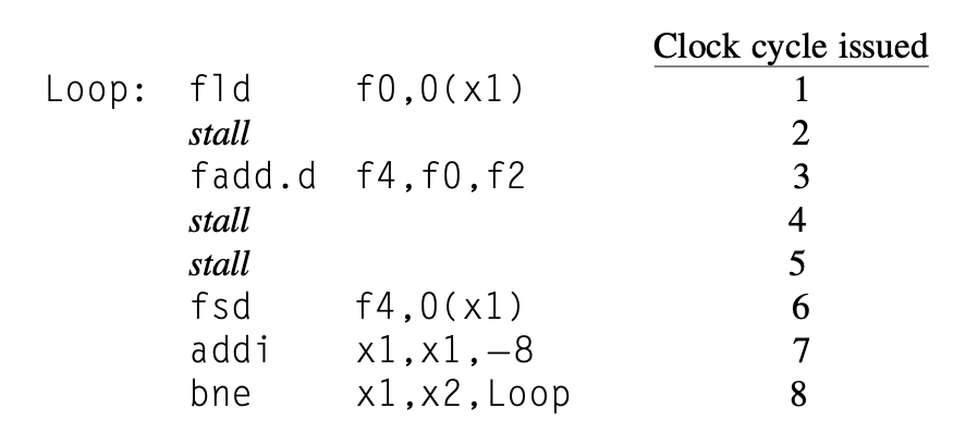
However, if scheduling is performed, one pause can be eliminated:
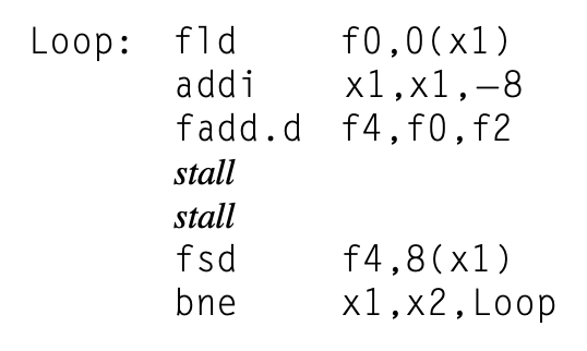
Here we moved the addi instruction to the position right after the fld instruction.
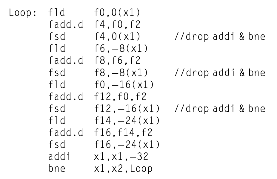
For the above example, there are actually only three instructions that operate on the array (fld, fadd.d, fsd). For the remaining two stalls, as well as the addi and bne instructions, we hope to eliminate them. To achieve this, a method called loop unrolling is introduced here:
Specifically, it involves copying multiple copies of the loop body and adjusting the code related to loop termination.
This method is most effective when each iteration of the loop is independent of the others, meaning there are no dependencies. In such cases, modern processors (superscalar, out-of-order execution) can execute these independent operations in parallel, thereby maximizing ILP.
Continuing with the above example, using loop unrolling, we copy four copies of the loop body. Here, it is assumed that the value of x1 - x2 is a multiple of 32, which also means the number of iterations is a multiple of 4. Redundant computations are eliminated while ensuring that no registers are reused.
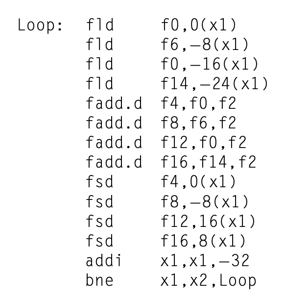
During unrolling, we merged the addi instructions and removed unnecessary duplicate bne instructions. The result is as follows:
Without scheduling, the above changes would not bring much improvement in performance. However, with scheduling, performance can be significantly enhanced (3.5 clock cycles per iteration), as shown in the results below:
Loop unrolling is usually done before compilation, so that redundant computations can be discovered and eliminated by the optimizer.
In real programs, we often do not know the upper bound of a loop. Suppose the upper bound is n , and we want to unroll the loop by copying the loop body k times. Loop unrolling generates a pair of consecutive loops: the first loop executes (n mod k) times with the original loop body, and the second loop is the unrolled loop body wrapped by an outer loop that iterates (n / k) times. For larger n , most of the execution time is spent within the unrolled loop body.
Loop unrolling improves performance by eliminating instruction overhead and discovering more computations that can reduce stalls through scheduling, but at the cost of significantly increasing code size.
Before obtaining the final unrolled code, we must make the following judgments and transformations:
Determine whether loop unrolling is useful by identifying independent loop iterations.
Use different registers to avoid unnecessary constraints caused by different computations using the same register.
Eliminate extra checks and branch instructions, and correct the loop termination and iteration code.
Determine whether loads and stores in the unrolled loop can be interchanged by observing whether they are independent across different iterations. This transformation requires analyzing memory addresses to ensure they do not point to the same location.
Preserve dependencies through code scheduling to ensure the results are consistent with the original code.
3.3 Advanced Branch Prediction
Correlating Branch Predictors
Improving prediction accuracy by observing the recent behavior of other branches.
This is a multi-branch code:
if (aa != 2) |
The corresponding RISC-V code is:
addi x3, x1, -2 |
It can be observed that the behavior of branch b3 is related to that of branches b1 and b2. If a predictor can only observe the behavior of a single branch, it will fail.
We refer to predictors that can leverage the behavior of other branches for prediction as correlating predictors or two-level predictors. Correlating predictors incorporate information about the behavior of recent branches to determine how to predict a given branch.
A typical correlating predictor has two bits:
First bit: If the last branch was not taken (NT), use it as a reference for the current branch.
Second bit: If the last branch was taken (T), use it as a reference for the current branch.
| Prediction Combination | First Bit | Second Bit |
|---|---|---|
| NT/NT | NT | NT |
| NT/T | NT | T |
| T/NT | T | NT |
| T/T | T | T |
The following figure illustrates the structure of a correlating predictor:
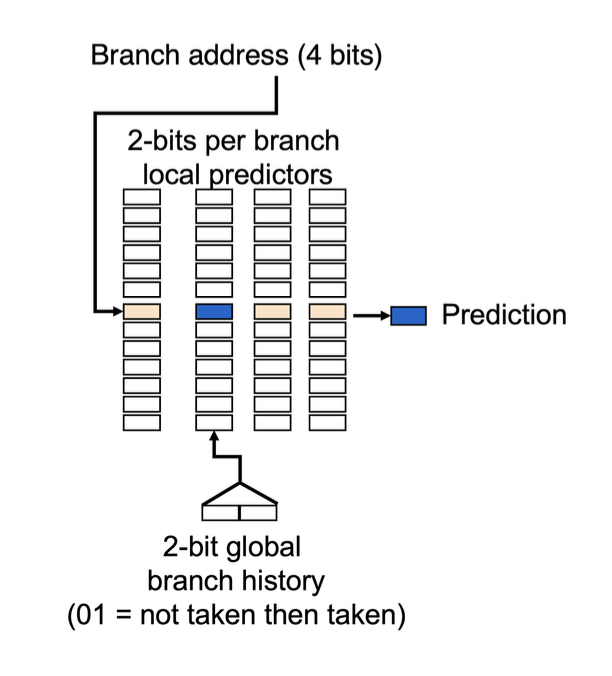
A correlating predictor can predict the behavior of the most recent branches to select from branch predictors, each being an -bit predictor for a single branch. This type of predictor can achieve a higher prediction rate than a 2-bit predictor with only a small increase in hardware. The structure of the correlating predictor is roughly as follows:
Among them, the total number of bits of the predictor is:
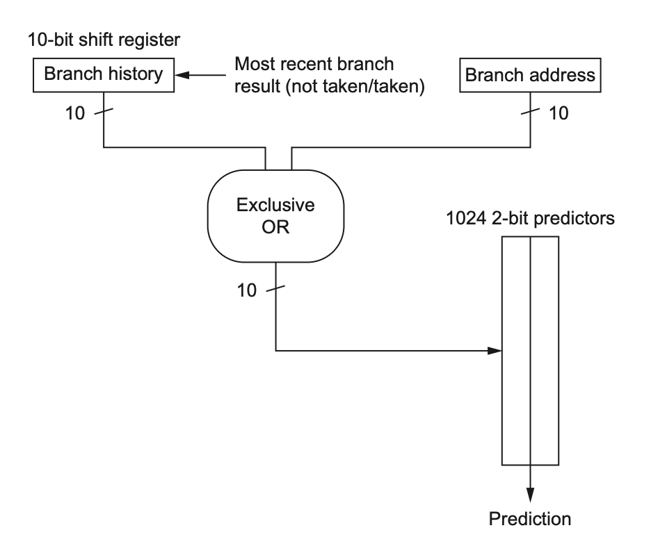
The reason hardware is simple is that the global history of the most recent branches can be recorded by an -bit shift register, where each bit indicates whether the corresponding branch was taken. The branch prediction buffer is then indexed by concatenating the low-order bits of the branch address with the -bit global history. By combining local and global information through concatenation (or a simple hash function), we can index a predictor table to achieve faster predictions than a 2-bit predictor. This type of predictor, which can combine local branch information with global branch history, is also known as an alloyed predictor or a hybrid predictor.
Tournament Predictors
Tournament predictors also utilize multiple predictors (global + local), but they select the best one from these predictors through a selector (essentially another type of alloy predictor or hybrid predictor). The general structure is as follows:
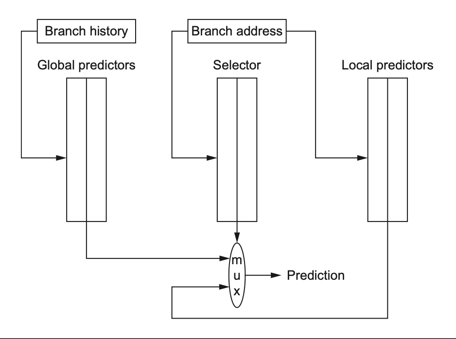
Global predictors use recent branch history to index the predictor.
Local predictors use the branch address as an index.
Tournament predictors achieve better accuracy at moderate sizes (8K-32K bits) and can effectively utilize a large number of prediction bits. They use a 2-bit saturating counter for each branch to select between the two predictors based on which one has been more accurate recently. In the original 2-bit predictor, this saturating predictor would make two incorrect predictions before switching to the better predictor.
Tagged Hybrid Predictors
A better-performing predictor, which references an algorithm similar to a branch prediction algorithm called PPM (Prediction by Partial Matching), uses a series of global predictors indexed by histories of different lengths. Its general structure is as follows:
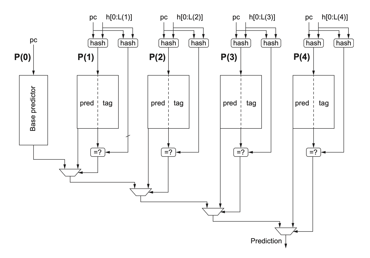
It can be seen that it has 5 prediction tables: . It uses the hash value of the PC and the most recent branches (stored in a shift register) to access . Apart from the different history lengths, another feature is the use of tags on the tables . Generally, small tags of 4-8 bits achieve the best results. Predictions from are used only when the tag matches the hash of the branch address and the global branch history. Each predictor in the example can be a standard 2-bit predictor. In practice, 3-bit counters perform slightly better than 2-bit counters.
The prediction for a given branch comes from the predictor with the longest branch history that has a matching tag. always matches because it has no tag, so if none of the other tables match, it provides the default prediction. The predictor also uses a 2-bit use field, which indicates whether the prediction has been used recently, and thus may be more accurate. All use fields are periodically reset to clear old predictions.
The disadvantage of this type of predictor is that it is overly complex to implement and may be slower (because checking multiple tags and selecting the prediction result takes time). Nevertheless, for multi-stage pipeline processors where the cost of branch misprediction is high, the advantages of this type of predictor clearly outweigh the disadvantages.
Larger predictors bring other issues, such as how to initialize the predictor—if done randomly, it requires a considerable amount of execution time. Therefore, some predictors use a valid bit to indicate whether an entry in the predictor has been set or is in an “unused state.”
3.4 Dynamic Scheduling
A technique that determines the order of instruction execution based on the current processor state and resource availability during program execution. Specifically, it reorders instruction execution through hardware to reduce stalls while maintaining (i.e., without altering) data flow and exception behavior.
A major limitation of simple pipeline technology is the use of in-order instruction issue and execution, meaning instructions are issued in program order. If an instruction stalls, subsequent instructions cannot proceed. Therefore, if there is a dependency between two closely spaced instructions, a hazard occurs, leading to a stall. If multiple functional units are available, they remain idle during the stall period. For the following instruction sequence:
fdiv.d f0, f2, f4 |
The first two instructions have a dependency, causing a stall. The third instruction has no dependency with the first two but still has to stall along with them. Therefore, we hope to continue executing the third instruction while the stall occurs.
To achieve this, we divide the issue process into two parts: checking for structural hazards and waiting for data hazards to resolve. Thus, we still use in-order instruction issue, but we want instructions to execute as soon as the processor’s operands are available. Such a pipeline performs out-of-order execution.
Out-of-order execution introduces the possibility of WAR and WAW hazards, which did not exist in the original pipeline. However, both types of hazards can be avoided through register renaming.
Out-of-order execution also complicates exception handling. A dynamically scheduled processor preserves exception behavior by delaying notification of an instruction’s exception until the processor knows that the instruction is the next one to be executed. Additionally, dynamically scheduled processors can produce imprecise exceptions, where the processor cannot guarantee that all instructions before the exception point have completed execution, and subsequent instructions may have been partially executed.
In contrast, precise exceptions strictly ensure that the instruction context at the exception point is fully reproducible. Modern processors typically convert imprecise exceptions into precise exceptions using mechanisms such as checkpoint recovery (similar to the ARIES algorithm in database systems) or reorder buffers (ROB).
To implement out-of-order execution, we divide the ID (decode) stage of the pipeline into two sub-stages:
Issue (IS): Decode the instruction and check for structural hazards (in-order issue)
Read Operands (RO): Wait until there are no data hazards, then read the operands (out-of-order execution)
The following techniques implement dynamic scheduling:
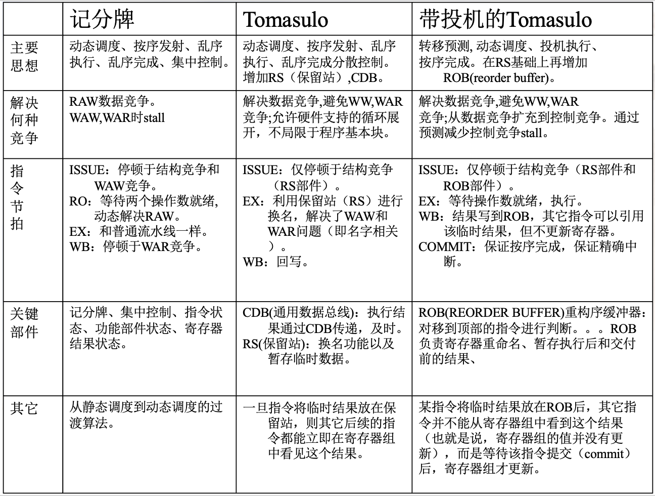
Scoreboarding: A technique that allows instructions to execute out of order when sufficient resources are available and there are no data dependencies.
Tomasulo’s Algorithm: A more sophisticated technique compared to scoreboarding, which handles anti-dependencies and output dependencies by dynamically renaming registers. Additionally, it can be extended to handle speculation.
These techniques will be detailed below.
Scoreboarding
A scoreboard is a technique that allows instructions to be executed out of order when sufficient resources are available and there are no data dependencies. Its goal is to maintain an execution rate of one instruction per clock cycle by executing instructions as early as possible. Therefore, when the next instruction to be executed is stalled, other instructions that do not depend on any currently active or stalled instructions can be issued and executed.
The following diagram shows the basic structure of a processor under the RISC-V architecture with a scoreboard:
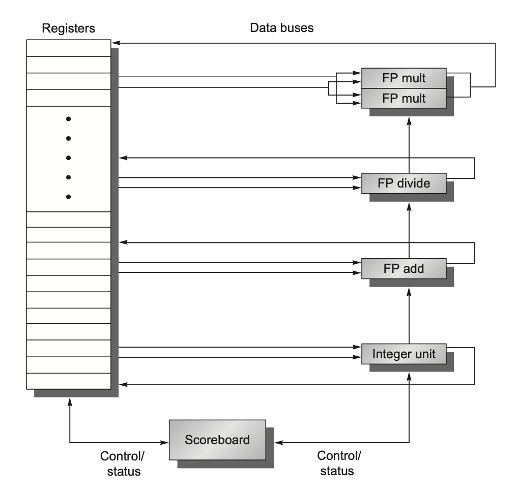
Each instruction (primarily for floating-point operations) goes through the following execution steps:
Issue:
- If the required functional unit is idle and no other instruction uses the same registers as the current instruction, the scoreboard issues the instruction to that functional unit and updates its internal data structures.
- By ensuring that no other active functional unit intends to write its result to the same destination register, WAW hazards are prevented.
- If a structural hazard or WAW hazard exists, instruction issuing (including other instructions) must be stalled until these hazards are resolved.
- When issuing is stalled, the buffer between the IF (instruction fetch) and issue stages will be filled. If the buffer holds only a single entry, IF can stop immediately; if the buffer is a queue capable of holding multiple instructions, IF stops only when the queue is full.
Read Operands:
- The scoreboard monitors the availability of source operands.
- If no previously issued active instruction intends to write to a source operand, that operand is available. The scoreboard then tells the functional unit that it can read the operand from the register and proceed.
- At this step, the scoreboard dynamically resolves RAW hazards, and instructions may be sent to the execution stage out of order.
- This step, combined with the previous one, completes the function of the ID stage in the original RISC-V pipeline.
Execution:
- Once all operands are received, the functional unit begins execution.
- When the result is computed, it notifies the scoreboard of this completion.
- This step replaces the EX stage of the original RISC-V pipeline and may take multiple clock cycles for floating-point operations.
Write Result:
- Once the scoreboard knows that the functional unit has completed execution, it first checks for WAR hazards and, if necessary, stalls the instruction that has completed execution.
- An instruction that has completed execution cannot write its result temporarily if a prior instruction (issued before it) has not yet read its operands and that operand uses the same register as the result of the completed instruction.
- If no WAR hazard exists or it has been resolved, the scoreboard tells the functional unit to store the result in the destination register.
- This step replaces the WB stage of the original RISC-V pipeline.
Unlike a simple pipeline, this method ensures that once execution is complete, the instruction’s result is immediately written to the register file (assuming no hazards), thereby reducing pipeline latency. However, because the write result and read operand stages cannot overlap, the scoreboard method introduces an additional clock cycle. This overhead can be eliminated by adding buffers.
Based on its own data structures, the scoreboard controls the progress of instructions through each stage by communicating with the functional units. However, the limited number of source operand buses and result buses in the register file indicates potential structural hazards. Therefore, the scoreboard must ensure that the number of functional units allowed to read operands or write results in steps 2–4 does not exceed the available buses. The CDC 6600 addressed this by dividing its 16 functional units into 4 groups, providing each group with a data trunk (a set of buses), and stipulating that only one unit per group could read operands or write results per clock cycle.
In analyzing the scoreboard, we use the following three tables:
- Instruction Status Table: Records the stage and status of each instruction.
- Functional Unit Status Table: Records the following information:
- Busy: Whether the functional unit is idle.
- Op: The operation being executed.
- Fi, Fj, Fk: The registers corresponding to the operands.
- Qj, Qk: The source of the operands (functional unit).
- Rj, Rk: The readiness status of the operands.
- Register Status Table: If a register’s value is still being computed in a functional unit, it retains the operation number; once computed, the actual value is filled in.
Limitations of the Scoreboard:
- Degree of ILP: If we cannot find independent instructions to execute, the scoreboard is of little use.
- Size of the Issue Window: This factor determines how far ahead the CPU looks for parallelizable instructions.
- Number, Type, and Speed of Functional Units: These determine the frequency of stalls due to structural hazards.
- Presence of Anti-dependencies and Output Dependencies: Compared to RAW hazards, WAR and WAW hazards impose greater restrictions on the scoreboard because they cause stalls. RAW issues arise in any technique, but WAR and WAW hazards can be resolved using methods other than the scoreboard.
Tomasulo’s Algorithm
In a dynamically scheduled processor using the Tomasulo algorithm,
RAW hazards can be avoided by executing instructions as soon as their operands are available.
WAR and WAW hazards can be eliminated through register renaming. If enough registers are available, the compiler can implement this renaming.
In the Tomasulo algorithm, register renaming is implemented by reservation stations. These act as buffers for instructions waiting to be issued and associated with functional units (their physical properties are closer to those of registers). The basic idea here is that when an operand becomes available, the reservation station fetches and caches it, eliminating the need to retrieve the operand from a register. Additionally, waiting instructions specify the reservation station that will provide their inputs. When an instruction is issued, the register identifiers for the waiting operands are renamed to the names of the reservation stations, thereby achieving register renaming.
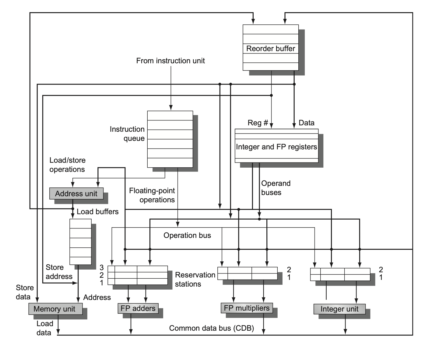
The following diagram shows the basic structure of a floating-point unit based on the Tomasulo algorithm:
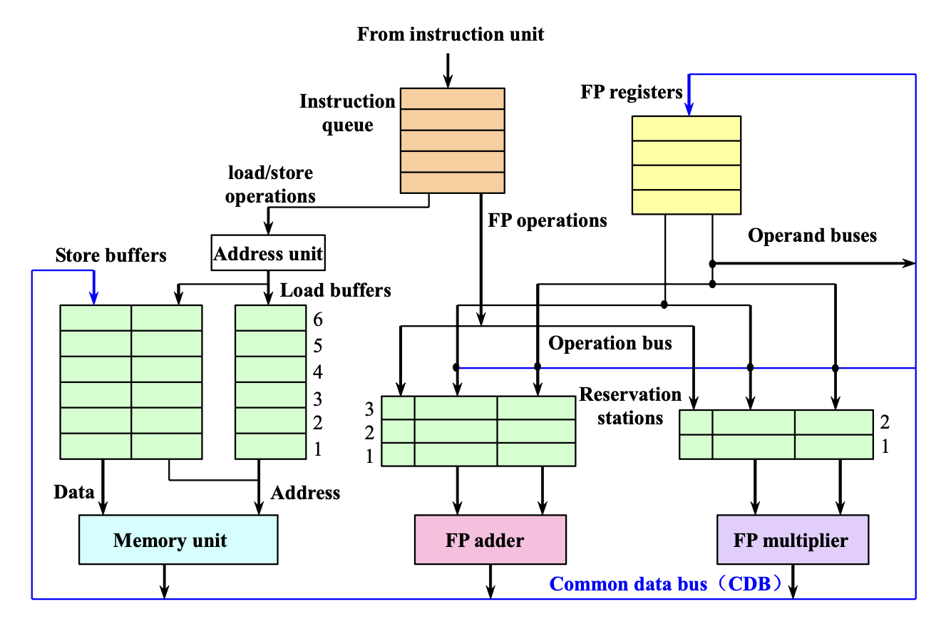
It contains a floating-point unit and a load-store unit.
Each reservation station holds an issued instruction that is waiting to be executed in a functional unit.
If the operand values of the instruction have already been computed, they are also stored; otherwise, the reservation station stores the names of the reservation stations that will provide the operand values.
The load buffer and store buffer respectively retain data or addresses coming from or going to memory, behaving similarly to reservation stations.
The floating-point registers are connected by a pair of buses from the functional units and one bus from the store buffer.
All results from functional units and memory are sent to the Common Data Bus (CDB), which passes through all components except the load buffer.
All reservation stations have a tag field used for pipeline control.
In the above processor, an instruction goes through the following three steps:
Issue (sometimes called dispatch):
Fetch the next instruction from the front of the instruction queue (FIFO order to maintain correct data flow).
If the reservation station matching the instruction is empty, issue the instruction and its operands (if currently in registers) to that reservation station.
If no empty reservation station is available, a structural hazard occurs, and instruction issuance stops until a reservation station slot is freed.
If an operand is not in a register, track the functional unit that will produce the operand value.
This step implements register renaming, eliminating WAR and WAW hazards in registers.
Execute:
If one or more operands are unavailable, the reservation station monitors the CDB, waiting for the operands to be computed.
When an operand becomes available, it is placed into any reservation station waiting for it.
When all operands for an operation are available, the operation is executed in the corresponding functional unit.
By delaying instruction execution until all operands are available, RAW hazards are avoided.
Sometimes multiple instructions may be ready in the same clock cycle and require the same functional unit; the unit must then choose among them. For example, the floating-point unit selects randomly, while the load-store unit is more complex.
Load and store operations require a two-step execution process:
Compute the effective address when the base register is available.
Then place it in the load or store buffer.
For loads, execution occurs immediately when the memory unit is available; for stores, execution waits until the value is sent to the memory unit.
To preserve exception behavior, instructions are not allowed to execute until branches that precede them in program order have completed.
If the processor records the occurrence of an exception but does not raise it, the instruction executes without stalling until it enters the “write result” stage.
Write Result:
When a result is available, write it to the CDB, then to registers and any reservation stations (including the store buffer) waiting for that result. This operation is called broadcasting.
Store operations are buffered in the store buffer until the value is stored and the store address is available, at which point the result is written to an available memory unit.
Data structures used to detect and eliminate hazards are attached to reservation stations, the register file, and the load and store buffers.
The retrieval of results from the bus by the CDB and reservation stations implements the forwarding (or bypassing) mechanism used in statically scheduled pipelines, but the dynamic scheduling method introduces an additional clock cycle delay.
When analyzing with Tomasulo’s algorithm, we use the following tables:
Instruction Status Table: Used only to help us understand the algorithm; it is not actually part of the hardware.
Reservation Station Table: Contains the status of each issued operation.
Register Status Table: Contains the number of the reservation station whose result needs to be stored in the register.
Each reservation station has 7 fields:
Op: The operation to be performed on source operands S1 and S2.
Qj, Qk: The reservation stations that will produce the corresponding source operands. A value of 0 indicates that the source operand is already available in Vj or Vk.
Vj, Vk: The values of the source operands. Note that for each operand, only one of the Q field or V field is valid. For loads, the Vk field is used to hold the offset field.
A: Holds information for memory address calculation for loads and stores. Initially, the immediate field of the instruction is stored here; after address calculation, the effective address is stored here.
Busy: Indicates whether the reservation station and its corresponding functional unit are occupied.
Advantages of Tomasulo’s Algorithm:
- Distribution of hazard detection units: This advantage comes from the use of distributed reservation stations and the CDB. If multiple instructions are waiting for the same result and all other operands for each instruction are ready, broadcasting the result via the CDB allows the instructions to be released simultaneously.
- Eliminating stalls caused by WAW and WAR hazards: This advantage is achieved by renaming registers in the reservation station and storing available operands in the reservation station.
Disadvantages of the Tomasulo Algorithm
Complex implementation, requiring a lot of hardware
Performance is also limited by the CDB
If different addresses are accessed, loads and stores can be safely executed out of order. However, if the same address is accessed, one of the following situations occurs:
If a load precedes a store in program order, swapping them results in a WAR hazard
If a store precedes a load in program order, swapping them results in a RAW hazard
Swapping two store instructions that access the same address results in a WAW hazard
3.5 Hardware-Based Speculation
The three key ideas of hardware speculation are:
Dynamic branch prediction: used to select the instructions to be executed
Speculation: allows instructions before control dependencies to be executed (i.e., the ability to undo the effects of incorrectly speculated instruction sequences)
Dynamic scheduling: handles the scheduling of different basic blocks
Hardware speculation follows the predicted data flow to decide when to execute instructions. This method of executing programs is called data flow execution: operations are executed immediately when operands become available.
An instruction is allowed to update the register file or memory only when it is no longer speculative. This step is called instruction commit.
The key idea behind implementing speculation is to allow instructions to execute out of order but force them to commit in order to prevent any irreversible actions. Therefore, when using speculation techniques, the process of completing execution must be separated from instruction commit; additional hardware buffers are needed to retain the results of instructions that have been executed but not yet committed. This buffer is called the reorder buffer (ROB), which is logically a FIFO queue but physically a buffer in memory. Since the ROB is similar to the store buffer, the store buffer is later merged into the ROB.
The following figure shows the structure of a processor that implements speculation and uses the Tomasulo algorithm:
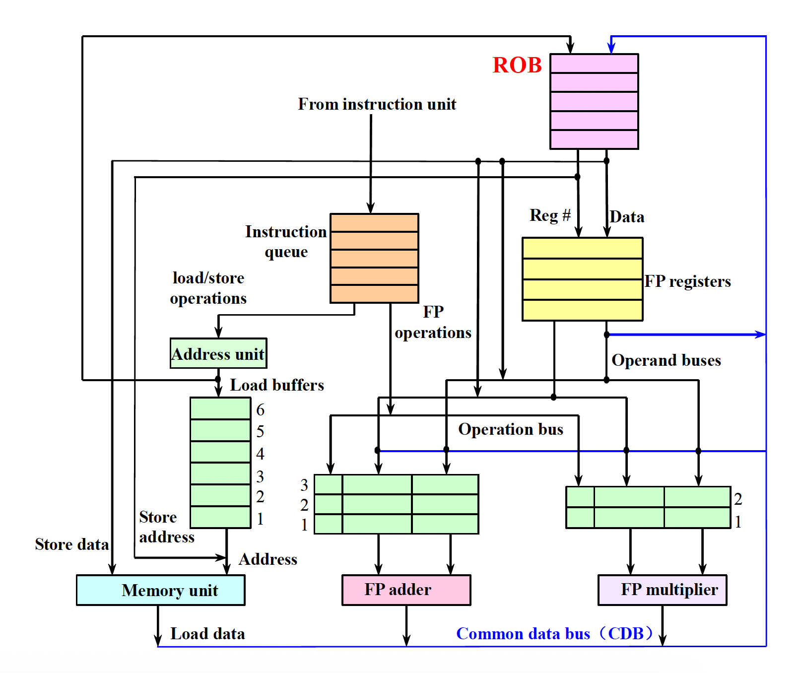
Each item in the ROB contains four fields:
Instruction type: Indicates whether the instruction is a branch instruction (no target result), a store instruction (target is a memory address), or a register operation (ALU operation and load instruction, target is a register).
Target field: Provides the register number (for ALU operations and load instructions) or memory address (for store instructions) where the instruction result should be written.
Value field: Holds the value of the instruction result until the instruction is committed.
Ready field: Indicates whether the instruction has completed execution and the value is ready.
Although the function of register renaming in the reservation station is now handled by the ROB, the reservation station still provides a buffer for operations from issue to execution. Since each instruction must have a position in the ROB before being committed, we use the ROB entry number to tag the result, and this tag must be trackable by the reservation station.
Now, instruction execution is divided into four steps:
Issue:
Fetch an instruction from the instruction queue.
If there is an empty reservation station and an empty ROB entry, issue the instruction.
If the operands are available in the registers or ROB, send them to the reservation station.
Update control entries to indicate that the buffer is in use.
The ROB entry number allocated for the result is also sent to the reservation station, so that when the result is placed on the CDB, this number can be used to tag the result.
If the reservation station or ROB is full, stop issuing instructions until a free entry becomes available.
Execute:
If one or more operands are unavailable, monitor the CDB and wait for the operands to be computed.
When all operands for an operation are available, execute the operation.
This stage may take multiple clock cycles.
Write Result:
When the result is available, write it (along with the ROB tag) to the CDB, then from the CDB to the ROB and to any reservation stations waiting for the result.
For store instructions, if the store value is available, write it to the value field of the ROB entry; if not, monitor the CDB until the value is broadcast.
Commit: There are three cases:
Normal commit (when the instruction reaches the head of the ROB and the corresponding value is in the buffer): The processor updates the register with the instruction execution result and removes the instruction from the ROB.
Commit store instruction: Similar to the previous case, but updates memory instead of registers.
Mispredicted branch instruction (i.e., incorrect speculation): Clear the contents of the ROB and restart with the correct instruction after the branch (rollback). Incorrect predictions significantly impact processor performance, so careful consideration must be given to all aspects of branch handling, including prediction accuracy, misprediction detection latency, and misprediction recovery time.
The processor only identifies and handles exceptions when it is ready to commit. If a speculative instruction triggers an exception, the exception is recorded in the ROB. If a branch misprediction occurs and the instruction has not yet been executed, the exception is cleared along with the other contents of the ROB. However, if the instruction has already reached the head of the ROB, we know that the instruction is no longer speculative and the exception has genuinely occurred, so it should be handled as soon as possible. Therefore, the Tomasulo algorithm combined with the ROB achieves precise interrupt capability.
Conclusion:
3.6 Multiple Issue
To further improve performance, we aim to reduce the CPI to below 1, which means multiple instructions need to be issued within a single clock cycle. Therefore, this section discusses the design of multi-issue processors, which include the following types:
Statically scheduled superscalar processors
- The number of instructions issued per clock cycle varies
- Assuming a maximum limit of n, such a processor is referred to as n-issue
- Can be implemented with static scheduling by the compiler or dynamic scheduling using the Tomasulo algorithm
- This approach is currently the most successful for general-purpose computing
VLIW (Very Long Instruction Word) processors
- A fixed number of instructions (4-16) are issued per clock cycle, formatted as a single large instruction or a fixed instruction packet with parallelism
- Parallelism among instructions within a packet is explicitly represented
- Statically scheduled by the compiler
- Successfully used in digital signal processing and multimedia applications
Dynamically scheduled superscalar processors
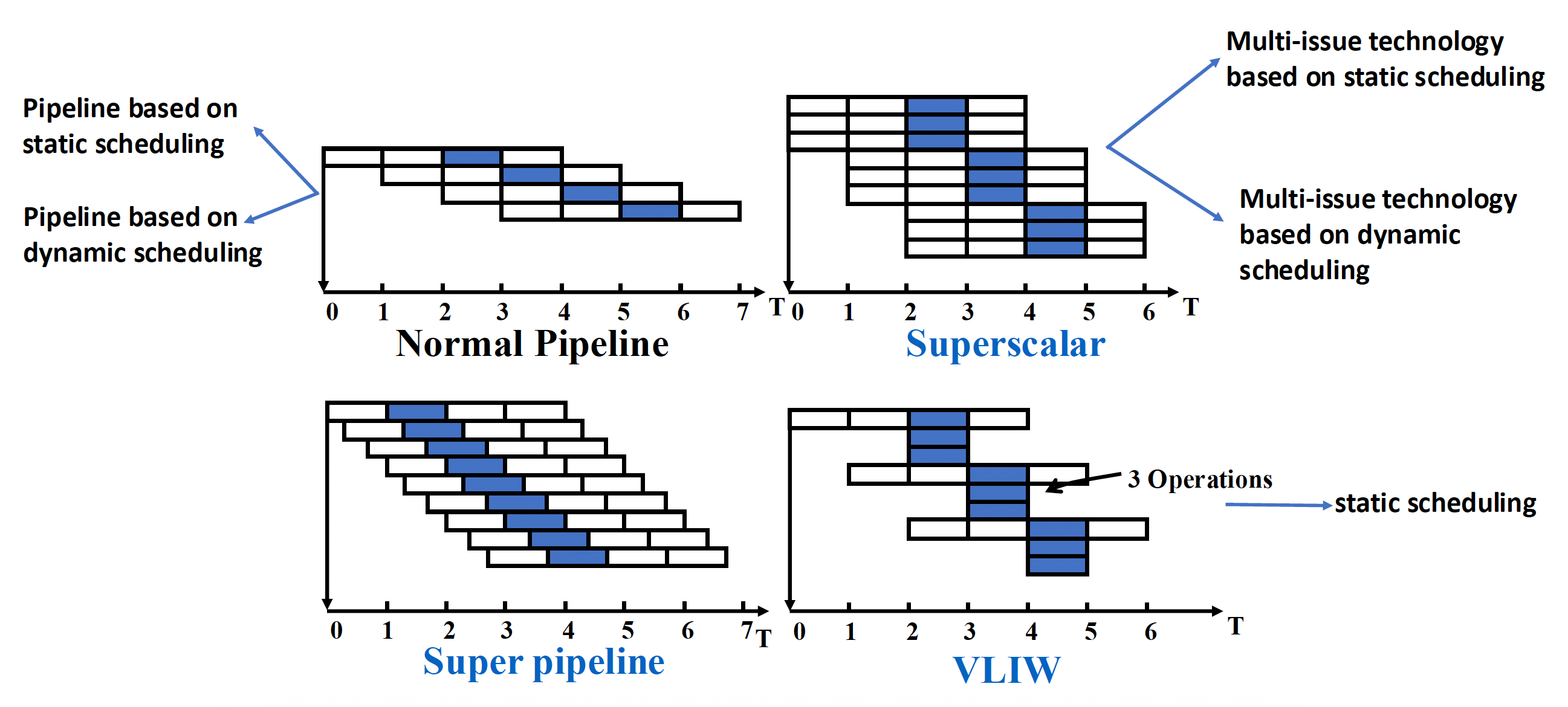
Summary: Five Basic Methods for Implementing Multi-Issue Processors
Using Static Scheduling
Let us first consider a statically scheduled superscalar processor:
Instructions are issued in order, and conflict detection is performed at the time of instruction issue. In the current instruction sequence, there are no data conflicts or close conflicts.
The outgoing component detects structural and data conflicts, typically implemented in two stages:
Stage 1: Perform conflict detection within the outgoing package and select instructions that can be issued first.
Stage 2: Check whether these selected instructions conflict with instructions currently being executed.
The RISC-V approach to superscalar implementation:
Assume 2 instructions are issued per clock cycle (64 bits): 1 integer instruction + 1 floating-point instruction. This parallelism keeps the increase in hardware manageable (load, store, and branch instructions are all considered integer instructions).
Also assume that floating-point instructions require 2 clock cycles to execute.
Floating-point load and store instructions use integer hardware, which increases access conflicts for floating-point registers. A mitigation method is to increase the number of read/write ports for floating-point registers.
Now consider VLIW:
Multiple independent functional units are used, and multiple operations are packed into a very long instruction, or instructions within a packet satisfy the same constraints.
The instruction word is divided into multiple fields, called operation slots, which can directly and independently control a functional unit.
All processing and instruction scheduling are handled by the compiler.
Since the advantages of VLIW increase with higher issue rates, we consider processors with wider issue widths.
To keep functional units busy, sufficient parallelism in the code is required, which can be achieved through loop unrolling and code scheduling as previously introduced. If the unrolled code is straight-line code (no branches), local scheduling techniques applied to a single basic block can be used. If parallelism requires scheduling code across branches, more complex global scheduling algorithms must be employed.
The VLIW model has some technical and logical issues:
Increase in code size. Solutions include: software scheduling that enhances parallelism through extensive loop unrolling; adopting smarter encoding methods; compressing instructions in memory and decompressing them when loading into the cache.
Limitations of lockstep operation: Any stall in a functional unit pipeline causes the entire processor to stall, as all functional units must remain synchronized (in modern processors, functional units operate more independently, and the compiler is used to avoid hazards at issue time, while hardware checks allow out-of-sync execution of instructions).
Insufficient binary code compatibility, making migration between different implementations difficult.
Using Dynamic Scheduling and Speculation
现在我们将动态调度、多发射和推测这三项技术结合起来,就可以得到一个和现代微处理器很像的微架构。为了便于后续讨论,我们仅考虑每时钟周期内发射两条指令的发射率。下图展示了带推测的多发射处理器的基本组织:
The difference from the previous organization chart is that certain lines are bolded to support multiple issue; the components remain unchanged.
The key lies in allocating reservation stations and updating pipeline tables.
Completing the above steps within half a clock cycle allows two instructions to be processed in one clock cycle, but this method is difficult to scale to more instruction issues.
Establishing the necessary logic to handle two or more instructions simultaneously (including any possible dependencies between them).
In dynamically scheduled superscalar processors, the issue stage is one of the most fundamental bottlenecks.
We can derive the basic strategy for issuing n instructions per clock cycle:
Allocate a reservation station and a reorder buffer entry for each instruction that may be in the next issue packet. This can be done before the instruction type is determined; specifically, n available ROB entries can be used to pre-allocate space sequentially for the instructions in the packet, ensuring there are enough available reservation stations to issue the entire packet.
Analyze the dependencies among all instructions in the issue packet.
If an instruction in the issue packet depends on a preceding instruction within the same packet, update the reservation station of the dependent instruction using the allocated ROB tag. Otherwise, update the reservation station of the instruction being issued using the existing reservation station and ROB.
The above process must be completed within a single clock cycle, making it quite complex.
3.7 Advanced Techniques for Instruction Delivery and Speculation
Increasing Instruction Fetch Bandwidth
In a high-performance pipeline, especially in the case of multiple issue, branch prediction alone is not sufficient. It is also necessary to deliver a high-bandwidth instruction stream.
A multiple-issue processor requires that the average number of instructions fetched per clock cycle is at least as large as the average throughput. Fetching instructions not only requires a sufficiently wide path in the instruction cache, but the most challenging aspect is handling branches. The following will introduce some methods for dealing with branches.
Branch-Target Buffers
If an instruction is a branch instruction and we already know the next PC value, the branch penalty is reduced to zero. The branch prediction cache used to store the predicted address of the next instruction after a branch is called a branch-target buffer, and its general structure is as follows:
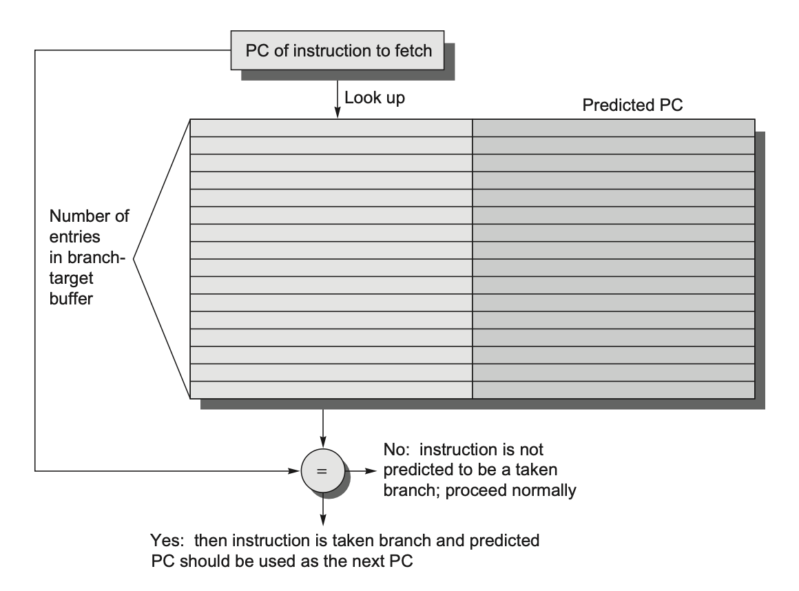
Since the branch-target buffer predicts the address of the next instruction and must send it out before decoding the instruction, we must know whether the fetched instruction is predicted to be a taken branch. If the PC value of the fetched instruction matches the address in the prediction buffer, then the corresponding predicted PC is used as the next PC.
The following shows the steps of the branch-target buffer when processing instructions:
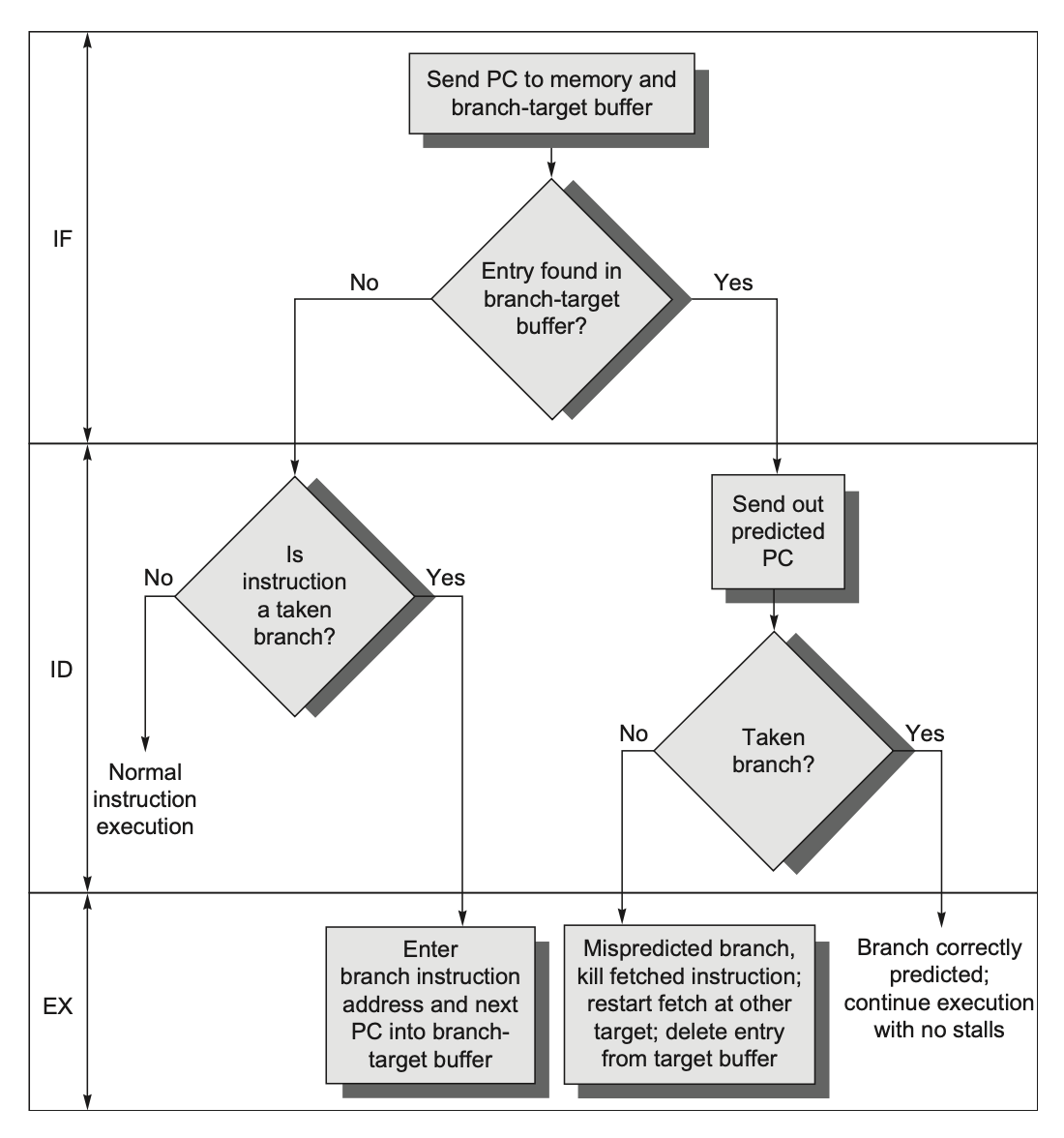
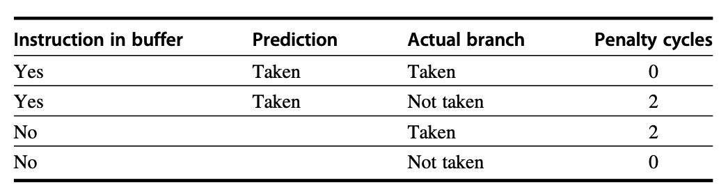
The table below shows various scenarios during branch prediction:
Specialized Branch Predictors
The next challenge we face is predicting indirect jumps, where the target address changes at runtime.
To overcome this issue, some designs use a small return address buffer that operates on the stack. This structure caches the most recent return addresses, pushing the return address onto the stack when a procedure is called and popping it when returning. If the buffer is large enough, it can perfectly predict return addresses.
To meet the demands of multi-issue processors, many designers choose to implement integrated instruction fetch units as separate autonomous units that supply instructions to the pipeline. This unit integrates the following functions:
Integrated branch prediction: The branch predictor is part of the instruction fetch unit and continuously predicts branches to drive the IF stage of the pipeline.
Integrated prefetching: To deliver multiple instructions in a single clock cycle, the instruction fetch unit may need to fetch instructions in advance. This unit automatically manages instruction prefetching, integrating it with branch prediction.
Instruction memory access and buffering: The instruction fetch unit uses prefetching to hide the cost of cache block crossing (?). Additionally, this unit provides buffers to supply instructions to the issue stage.
Implementation Issues and Extensions of Speculation
Speculation Support: Register Renaming v.s. Reorder Buffers
An alternative to ROB is to use a larger set of register files combined with register renaming technology, which is also based on the Tomasulo algorithm. In the Tomasulo algorithm, at any point during execution, the values of architecturally visible registers are contained within the register file and reservation stations. If speculation techniques are used, register values may also temporarily reside in the ROB.
During instruction issue, the renaming process maps the names of architectural registers to physical register numbers, allocating a new unused register as the target. Through this method, WAW and WAR hazards can be avoided, and speculative recovery can be handled because the physical register holding the instruction’s target does not become an architectural register until the instruction commits. The renaming map is a simple data structure that provides the current physical register number corresponding to a given architectural register, a function performed by the register status table in the Tomasulo algorithm.
Compared to the ROB method, the advantage of the renaming method is that it slightly simplifies instruction commit, as it records the non-speculative mapping between architectural register numbers and physical register numbers and releases the physical registers that stored the old values of architectural registers. However, register renaming makes releasing registers more complex—a physical register corresponds to an architectural register until the architectural register is overwritten, which causes the renaming table to point elsewhere. Therefore, if a physical register is not used as a source and is not assigned to a corresponding architectural register, it needs to be reclaimed and reallocated. A simpler approach is to have the processor wait for other instructions writing to the same architectural register to commit, a method used by most recent superscalar processors.
The issue logic needs to retain enough physical registers for a complete issue packet.
The issue logic needs to determine the dependencies within the issue packet. If no dependencies exist, the register renaming structure is used to determine the physical registers, saving the results of current or future instruction dependencies. When there are no dependencies within the issue packet, the results from previous issue packets and the register renaming table will have the correct register numbers.
If an instruction depends on another instruction within the same packet that precedes it, a pre-reserved register needs to be used to update the information of the issued instruction.
The Challenge of More Issues per Clock
Only when precise branch prediction and speculation are adopted will we consider increasing the issue rate; otherwise, it becomes difficult to scale the issue rate due to the need to resolve branch issues. Increasing the issue rate also makes the issue stage and the commit stage (which is essentially the dual of the issue stage) more complex.
How Much to Speculate
One major benefit of speculation is the ability to hide events that cause pipeline stalls, such as cache misses. However, the downside of speculation is that it consumes time and energy, and recovering from incorrect speculation can degrade performance. Additionally, to achieve a higher instruction execution rate through speculation, the processor must have additional resources, which require more chip area and power. Finally, if speculation causes an exception to occur (one that would not have occurred without speculation), it can lead to significant performance loss.
To maintain the advantages of speculation, most speculative pipelines only allow low-cost exception events to be handled in speculative mode. If a high-cost exception event occurs, the processor will wait until the instruction causing the event is no longer speculative before handling it. Although this may reduce performance for some programs, it avoids significant performance loss in others.
Speculating Through Multiple Branches
Speculating on multiple branches simultaneously can bring benefits in the following situations:
- Very high branch frequency
- Significant branch clustering
- Long latency of functional units
Challenge of Energy Efficiency
It is speculated that if the reduced execution time can outweigh the increase in average power consumption it brings, then the total energy consumption will decrease.
Address Aliasing Prediction
Address aliasing prediction is a technique used to predict whether two store instructions, or a store instruction and a load instruction, access the same address. If they access different addresses, the two can be safely swapped; otherwise, the instructions must access memory addresses in order (which may require waiting for some time).
Since we do not need to predict the specific address value, only whether the two values conflict, accurate prediction can be achieved with a small predictor.
Address aliasing prediction is also a simple and restricted form of value prediction. It attempts to predict the value generated by an instruction. If accurate enough, it can eliminate data flow constraints to achieve a higher ILP rate.
3.8 Cross-Cutting Issues
Hardware v.s. Software Speculation
To extend speculation, it must have the ability to resolve memory access ambiguities. In hardware-based methods, this capability is difficult to achieve at compile time; however, through hardware, it can be dynamically realized at runtime, allowing load instructions to be moved ahead of store instructions. If this method is used improperly, the recovery overhead may outweigh the benefits.
For most integer programs, hardware-based speculation performs better when control flow is unpredictable and when hardware-based branch prediction completes before software-based branch prediction.
Hardware-based speculation can maintain a fully precise exception model, even for speculative instructions. Recent software-based methods can also achieve this.
Compiler-based methods have the ability to observe longer code sequences, potentially achieving better code scheduling than purely hardware-based implementations.
Hardware-based speculation without dynamic scheduling does not require different code sequences to achieve good performance across different implementations of the same architecture.
The main drawback of hardware-based speculation is its complexity, requiring additional hardware resources.
Speculative Execution and the Memory System
Registers that support speculative execution and conditional instructions may generate illegal addresses, thereby affecting processor performance—something that does not occur in processors without speculative execution. Therefore, the memory system must identify speculatively executed and conditionally executed instructions and suppress the corresponding exceptions. Moreover, we must not allow such instructions to cause cache stalls or invalidations, so the processor must be paired with a non-blocking cache.
3.9 Multithreading: Exploiting Thread-Level Parallelism to Improve Uniprocessor Throughput
This mainly introduces multithreading on a single processor.
Multithreading is a technique that leverages thread-level parallelism (TLP) to improve throughput by hiding parallelism. It is actually a cross-domain technology, related to pipelining, superscalar processing, GPUs, and multiprocessors.
A thread is similar to a process, with its own state and program counter (PC), but multiple threads share the same address space of a process, allowing them to easily access each other’s data. Thus, multithreading enables a single processor to hide pipeline and memory latency by quickly switching between threads without performing a process switch.
The following introduces some major hardware multithreading methods:
Fine-grained multithreading:
- Switches between threads every clock cycle, interleaving the execution of instructions from multiple threads.
- Typically uses a round-robin approach, skipping any stalled threads.
- Advantages: It can hide throughput losses caused by both short and long stalls, as instructions from other threads can be executed when one thread stalls.
- Disadvantages: It slows down the execution of a single thread because even if a thread is ready to execute without stalling, its instructions are delayed by instructions from other threads.
Coarse-grained multithreading:
- An alternative to fine-grained multithreading.
- Switches to another thread only when a thread encounters a high-cost stall, such as a level 2 or level 3 cache miss.
- Advantages: It avoids the overhead of frequent thread switching and hides long-latency events without slowing down the execution of any single thread.
- Disadvantages: Its ability to overcome throughput loss is limited, especially for shorter stalls; due to pipeline startup costs, there may be idle time in the pipeline when a thread stalls and switches to a new thread.
Simultaneous multithreading (SMT):
- The most common implementation.
- A variant of fine-grained multithreading that naturally arises when implemented on a multi-issue, dynamically scheduled processor.
- SMT uses thread-level parallelism to hide long-latency events in the processor, thereby increasing the utilization of functional units.
- Key point: The essence of SMT lies in register renaming and dynamic scheduling, allowing multiple instructions from independent threads to be executed without considering dependencies between them; dependency resolution is handled by dynamic scheduling capabilities.
- SMT allows the processor to execute instructions from multiple different threads in the same clock cycle.
Chapter 4 Data-Level Parallelism in Vector, SIMD, and GPU Architectures
In this chapter, we will explore some common techniques for data-level parallelism. Among them, the most well-known is SIMD (Single Instruction, Multiple Data), which is widely used in scientific computing for matrix operations, media-oriented image and audio processing, and machine learning algorithms. Compared to MIMD, SIMD is more energy-efficient, making it suitable for personal mobile devices and servers. However, the biggest advantage of SIMD is that programmers can still think in a sequential manner while the underlying hardware accelerates computations through parallelism.
This chapter mainly covers three major topics, all of which are variants of SIMD:
- Vector architecture
- Multimedia SIMD instruction set extensions
- Graphic processing units (GPUs)
The latter two are closely related to vector architecture, so we will first study the principles and implementation of vector architecture.
4.1 Vector Architecture
The general principle of vector architecture can be summarized as follows: it retrieves sets of data elements scattered in memory, places them in a large sequential register file, performs operations on the data within the register file, and finally scatters the results back into memory.
A single instruction operates on multiple vector data, resulting in multiple register-to-register operations on independent data elements.
Acting as compiler-controlled buffers, these register files can hide memory latency and make efficient use of memory bandwidth.
The power wall has led architects to value architectures that can achieve high performance without incurring the high costs of out-of-order superscalar processors. Vector architecture meets this requirement—by simply using vector instructions on a simple scalar processor, performance can be improved.
Classification of vector architectures
Memory-memory vector processor: All vector operations are performed between memory locations.
Vector-register processor: All vector operations (except loads and stores) are performed within vector registers. (The vector architectures introduced later belong to this category.)
One characteristic of vector processors is that elements within a vector are rarely correlated during operations. However, incorrect vector processing can lead to correlation problems and frequent function switches. In vector pipelines, we need to consider how to handle vectors to improve pipeline efficiency. Below are some solutions:
Horizontal processing method: Vector calculations are performed row by row from left to right.
Vertical processing method: Vector calculations are performed column by column from top to bottom.
Vertical and horizontal processing method (group processing method): Combines the previous two methods.
The following example compares the effects of these three methods—assuming we need to compute D = A * (B + C), where A, B, C, and D are vectors of length N.
Horizontal processing method
Calculation process: d1 <- a1 * (b1 + c1) // d2 <- a2 * (b2 + c2) … dN <- aN * (bN + cN)
A loop program is constructed to handle: ki <- bi + ci // di <- ai * ki
Data dependencies: N times, function switches: 2N times
Issue: When computing each part, RAW dependencies occur, resulting in low pipeline efficiency. If a static multi-functional pipeline is used, the pipeline must switch frequently, and its throughput becomes smaller than that of serial execution. Therefore, this method is not suitable for vector processors.
Vertical processing method
Calculation process: K <- B + C // D <- A * K
Data dependencies: 1 time, function switches: 2 times
Requires a memory-to-memory processor structure: The source and destination vectors of vector instructions must be stored in memory, and the immediate results of operations must also be sent back to memory.
Group processing method
Divides the vector into multiple groups, processes them vertically, and then processes each group sequentially.
Let N = S * n + r, where N is the vector length, S is the number of groups, n is the group length, and r is the remainder (if treated as a complete group, the number of groups is S + 1).
Calculation process: d_{1-n} <- a_{1-n} * (b_{1-n} + c_{1-n}) // d_{n+1-2n} <- a_{n+1-2n} * (b_{n+1-2n} + c_{n+1-2n}) … d_{Sn+1-N} <- a_{Sn+1-N} * (b_{Sn+1-N} + c_{Sn+1-N})
Data dependencies: S+1 times, function switches: 2(S+1) times
Requires a register-to-register processor structure: Fast-access vector registers are set up to store source vectors, destination vectors, and intermediate results, connecting the input and output ends of the arithmetic unit to the vector registers to form a register-to-register type operation pipeline.
Vector pipeline processing structures vary by machine. Below, using the CRAY-1 as an example, some structural features of register-to-register vector pipeline processing machines are introduced.
The above diagram can be simplified and represented as follows:
The characteristics of the CRAY-1 vector processor include:
Each vector register Vi has a dedicated bus connecting to six vector functional units.
Each vector functional unit also has a bus that returns the operation result to the vector register bus.
As long as there are no Vi conflicts or functional conflicts, each Vi and functional unit can work in parallel, greatly accelerating the processing of vector instructions.
Vi conflict: The source or result vector of each vector instruction uses the same Vi for parallel operation.
Read-write data dependency: V0 <- V1 + V2, V3 <- V0 * V4
Read data dependency: V0 <- V1 + V2, V3 <- V1 * V4
Functional conflict: Each vector instruction operating in parallel must use the same functional unit.
Example (both require the multiplication function): V3 <- V1 * V2, V5 <- V4 * V6
The second instruction begins execution only after the last part of the first instruction has been completed and the floating-point multiplication function is released.
The following methods can improve the performance of vector processors:
Establish multiple functional units and make them work in parallel: These units can operate in parallel and in a pipelined manner, thus forming multiple parallel operation pipelines.
Use vector chaining technology to accelerate the execution of a series of vector instructions: Chaining involves two related instructions (RAW). When there is no conflict between the functional components and the source vectors, the functional components can be chained for pipelined processing, thereby achieving faster execution. Its essence is the result of introducing the pipeline concept into the vector execution process.
Adopt recycling mining technology to accelerate loop processing.
Segmented vector processing: When the vector length exceeds the length of the vector register, the long vector must be divided into multiple fixed-length segments, which are then processed in a loop, with each loop handling only one segment. This method is controlled by system hardware and software and is transparent to the programmer.
Use a multiprocessor system to further enhance performance.
RV64V Extension
Here, “RV64V” refers to the RISC-V base instructions plus the vector instruction extension.
Vector registers:
RV64V has 32 vector registers, each 64 bits in size, storing one vector.
The vector register file must provide enough ports to supply the vector functional units; these ports allow a high degree of overlap between vector operations on different vector registers.
There are at least 16 read ports and 8 write ports, connected to the inputs and outputs of the functional units via a crossbar switch.
One method to increase register file bandwidth is to use multiple banks.
Vector functional units:
All units are fully pipelined and can start a new instruction every clock cycle.
The control unit detects hazards, including structural hazards in functional units and data hazards in register access.
As shown in the diagram above, only five functional units are provided here, but in this section, we focus only on the floating-point unit.
Vector load/store unit:
These units are also fully pipelined, ensuring a bandwidth of one word per clock cycle after the initial latency.
They can also handle scalar loads and stores.
A set of scalar registers:
These primarily provide data and computed addresses.
In RV64G, there are 31 general-purpose registers and 32 floating-point registers.
The reason RV64V adopts such dynamic register typing is because
If a traditional vector architecture were to support such a diverse combination of data types, it would require a large number of instructions, resulting in an instruction list spanning several pages.
Programs can disable unused vector registers, thereby allocating all vector memory to the vector registers for storing long vectors. The downside of this approach is that a larger state leads to slower context switch times. However, a beneficial side effect is that programs can disable unused registers, eliminating the need to save and restore them during context switches.
Implicit conversion of operands of different sizes can be achieved through register configuration, eliminating the need for explicit conversion via additional instructions.
Some vectors may be very long, requiring more than one vector register. In such cases, the following registers are used:
- vl: Vector length register, used when the vector length is not equal to mvl.
- vctype: Vector type register, which records the register type.
- pi: Predicate register, used for loops containing IF statements.
Through these vector instructions, the system can perform vector operations in multiple ways, including computing multiple elements simultaneously. This flexibility allows vector designs to use slow but wide execution units, achieving higher performance at lower power consumption. Additionally, the independence of elements in the vector instruction set enables functional unit scaling without the need for expensive dependency checks, as required in superscalar processors.
When a compiler generates a sequence of vector instructions, the code runs in vector mode for a significant amount of time, and such code is considered vectorized. Loop code can be vectorized when there are no dependencies between iterations, a condition known as loop-carried dependencies.
Another difference between RV64G and RV64V is the frequency of pipeline interlocks. Due to data dependencies, RV64G instructions experience many stalls. However, in vector processors, each vector instruction only stalls for the first element, after which subsequent elements flow smoothly through the pipeline. This type of element-dependent operation is called chaining.
Vector Execution Time
The execution time of a vector operation sequence depends on the following factors:
- The length of the operand vectors
- Structural hazards between operations
- Data hazards
All modern vector computers have vector functional units with multiple parallel pipelines (called lanes), capable of producing two or more results per clock cycle. However, some functional units are not fully pipelined. For the sake of discussion:
- Our RV64V implementation has only one lane, with an initiation rate of one element per clock cycle for a single instruction. Therefore, the execution time (in clock cycles) of a single vector instruction is approximately equal to the vector length.
- Convoy: A group of vector instructions that can be executed together.
- These instructions must not contain any structural hazards; if such hazards exist, they must be serialized and executed in different convoys.
- We also assume that instructions within a convoy must complete execution before other instructions begin.
- Chaining allows RAW dependency hazards within the same convoy, as vector operations can begin execution as soon as source operands become available—the result from the first functional unit in the chain is forwarded to the second functional unit. In practice, we implement the concept of chaining by allowing the processor to read and write specific vector registers simultaneously.
- Chime: The time required to execute one convoy.
- Therefore, executing m convoys takes m chimes; if the vector length is n, the total number of clock cycles is m × n.
- Since this calculation ignores certain processor-specific overheads (many of which depend on vector length) and the limitation of initiating multiple vector instructions in a single clock cycle, this approximate measurement is more accurate for long vectors.
- Additionally, the most significant overhead ignored by this method is the vector start-up time, which is the delay before the pipeline is fully filled and depends on the pipeline latency of the vector functional units.
Optimizations
Below are some optimization methods for improving performance or enabling more types of programs to run on vector architectures:
Multiple lanes: Allow the vector processor to process multiple elements of a vector in a single clock cycle.
Vector-length registers: Handle cases where the vector length does not equal the maximum vector length (which is most cases).
Predicate registers: Efficiently handle conditional statements, enabling more code to be vectorized.
Memory banks: Provide sufficient memory bandwidth for the vector processor.
Stride: Handle multidimensional matrices.
Gather-scatter: Handle sparse matrices.
Programming vector architecture.
Multiple Lanes
A key advantage of vector instruction sets is that they allow software to convey a large amount of parallel work to hardware through a single, relatively short instruction (which contains multiple independent operations and has the same encoding length as traditional scalar instructions). The parallel semantics of vector instructions make it possible to implement the execution of these element-wise operations using highly pipelined or parallel functional units. The diagram below illustrates how multiple parallel functional units can improve the performance of a vector addition instruction (right diagram; the left diagram shows only a single pipeline):
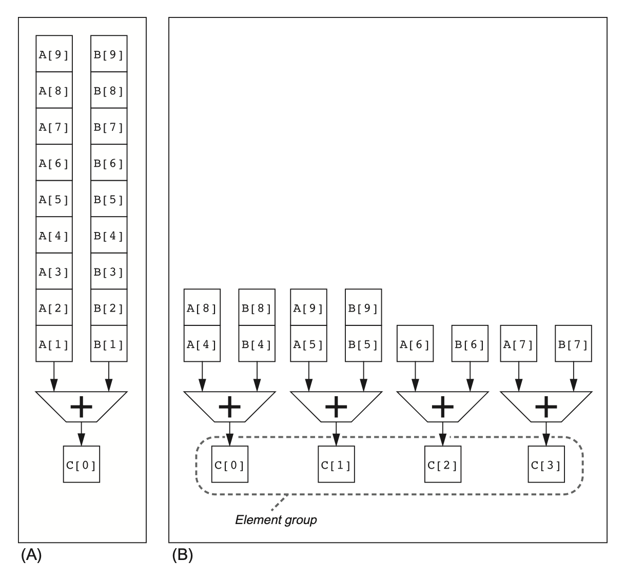
A property of the RV64V instruction set is that all vector arithmetic instructions only allow operations between element N of one vector register and element N of another vector register, thereby simplifying the design of parallel vector units—these units are structured as multiple parallel lanes, and increasing the number of lanes can enhance the peak throughput of the vector unit.
To fully leverage the advantages of multiple lanes, both applications and architectures must support long vectors; otherwise, execution proceeds too quickly, easily exhausting instruction bandwidth, requiring ILP to supply enough vector instructions.
Each lane contains a portion of the vector register file and one execution pipeline from each vector functional unit.
Each vector functional unit executes vector instructions at a rate of processing one element group per clock cycle in each lane that uses multiple pipelines (a group of elements that move together through the pipeline).
The first lane holds the first element (element 0) of all vector registers, and so on. This allocation allows the arithmetic pipelines within a lane to complete computations without communicating with other lanes, thereby reducing the cost of wiring and additional register file ports.
Furthermore, the multi-lane design can improve vector performance with only a small increase in control complexity and without modifying existing machine code; it also allows designers to trade off die area, clock rate, voltage, and power without sacrificing peak performance.
Vector-Length Registers
Add a vector length register vl, which controls the length of any vector operation, with its value not exceeding mvl. This parameter means that the length of the vector register can be increased later without modifying the instruction set.
However, if n is unknown at compile time and its value may exceed mvl, then strip mining technology is needed. It can generate code where the vector operation length does not exceed mvl.
Specifically, one loop handles any number of iterations that are multiples of mvl, while another loop handles the remaining iterations, with the number being less than mvl.
RISC-V provides a better solution: the setvl instruction writes a value less than mvl and the loop variable n into vl (or another register).
If the number of loop iterations exceeds
n, the loop can compute up tomvlvalues at once in the fastest case, sosetvlsetsvltomvl.If
nis less thanmvl, only the lastnelements should be computed in the final iteration of the loop, sosetvlsetsvlton.setvlalso writes to another scalar register to assist with subsequent loop management.
Predicate Registers
If a loop in a program contains an IF statement, it cannot be executed in vector mode (as described above) because the IF statement introduces control dependencies. Consider the following code:
for (i = 0; i < 64; ++i) |
This loop cannot be vectorized; however, if the inner loop can be executed when the iteration satisfies X[i] != 0, then the subtraction operation can be vectorized.
We refer to this extended capability as vector-mask control, while compiler designers call it IF-conversion. In RV64V, predicate registers store masks and provide conditional execution for each element operation in vector instructions. These registers use Boolean vectors to control the execution of vector instructions. When predicate register p0 is set, all vector instructions only operate on vector elements whose corresponding value in the predicate register is 1, while elements with a corresponding value of 0 remain unchanged. Similar to vector registers, predicate registers can be enabled and disabled. When enabled, their values are initialized to 1, meaning subsequent vector instructions will operate on all elements.
Although introducing additional registers incurs extra overhead, it eliminates branches and associated control dependencies, making conditional instruction execution faster (even if the registers sometimes perform unnecessary work).
Memory Banks
The behavior of vector load/store units is much more complex than that of arithmetic functional units—their initiation rate is not necessarily one clock cycle, because memory partition stalls can reduce effective throughput; and the startup penalty is much higher than that of typical functional units. To maintain the theoretical initiation rate, the memory system must be able to produce or receive large amounts of data by distributing accesses across multiple independent memory partitions.
Many vector computers support multiple loads and stores within a single clock cycle, and the memory partition cycle time is often several times the processor cycle time. To support multiple simultaneous accesses, the memory system requires multiple partitions and the ability to independently control partition addresses.
Most vector processors support the ability to load or store word data out of order, which requires support for independent partition addressing—simple memory interleaving cannot achieve this.
Most vector computers support multiple processors sharing the same memory system, so each processor will generate its own separate address stream.
Stride
The positions of adjacent elements in a vector in memory are not necessarily sequential. Consider the following matrix multiplication code:
for (i = 0; i < 100; ++i) |
We can vectorize the multiplication between each row of B and each column of D, using k as the index variable to perform strip mining on the inner loop. However, when memory is allocated for arrays, they are linearized, meaning that elements in the same row or column are not necessarily adjacent in memory. Taking the above C code as an example, since C uses row-major order, the elements of D accessed during iteration are spaced 800 bytes apart (100 elements per row * 8 bytes). Therefore, we need a technique that can access vector elements that are not adjacent in memory.
Stride: The distance between elements to be gathered into a single vector register.
- In the above example, the stride of matrix D is 100 double-precision words, while the stride of B is 1 double-precision word; if column-major order were used, the two would be swapped.
When a vector is loaded into a vector register, it appears to have logically adjacent elements. Thus, vector processors can handle non-unit strides (stride > 1) through vector load and store operations with stride capability. This ability to access non-sequential memory locations and reshape them into a compact structure is a major advantage of vector architectures.
Since the stride may be unknown at compile time, just like the vector length, we can place the vector stride in a general-purpose register. The RV64V instruction vlds (load vector with stride) then loads the vector into a vector register; for storage, there is a corresponding vsts (store vector with stride) instruction.
When multiple accesses compete within a single partition, a memory partition conflict occurs, causing one access to stall. A partition conflict is considered to occur when the following relationship holds (LCM stands for least common multiple):
Gather-Scatter
In sparse matrices, vector elements are typically stored in some compact form and require indirect access. Suppose there is a simplified sparse structure, with the corresponding code as follows:
for (i = 0; i < n; ++i) |
This code implements sparse vector summation on arrays A and C, using index vectors K and M to specify the non-zero elements in A and C. Here, A and C must have the same number (n) of non-zero elements, and K and M must also be of the same size.
The basic mechanism for supporting sparse matrices is the use of gather-scatter operations with index vectors. The goal of these operations is to support the movement of sparse matrices between compressed and normal representations.
The gather operation takes an index vector and retrieves a vector of elements from addresses obtained by adding the base address to the offsets given in the index vector. The result is a dense vector in a vector register.
After performing operations on the elements of the dense vector, the sparse vector can be stored in expanded form using the scatter operation, while employing the same index vector.
The corresponding instructions provided by RV64V are vldi (load vector indexed or gather) and vsti (store vector indexed or scatter).
Although indexed loads and stores can be pipelined, they are slower than their non-indexed counterparts because memory partitions cannot be determined at the start of the instruction, and the register file must also support communication between vector unit lanes to enable gather and scatter operations.
Each element in gather and scatter operations has an independent address, so they cannot be processed in groups and may cause multiple conflicts in the memory system. Therefore, even in systems with caches, individual accesses can result in significant latency.
Programming Vector Architecture
One advantage of the vector architecture is that the compiler can inform the programmer at compile time whether a piece of code can be vectorized, often providing hints for code that cannot be vectorized. This allows domain experts to know how to improve performance by modifying the code or by telling the compiler that the code is fine. It is this dialogue between the compiler and the programmer that simplifies programming on vector computers.
However, the main factor affecting whether a program runs in vector mode is the program itself: whether loops have true data dependencies, or whether they can be restructured to avoid such dependencies. The choice of algorithm and the way it is coded also influence this factor.
4.2 SIMD Instruction Set Extensions for Multimedia
SIMD multimedia extensions originated from a simple discovery: many media applications process data types that are narrower than the 32-bit data types that processors were originally optimized for.
Similar to vector instructions, SIMD instructions specify the same operation on vector data; the difference is that SIMD tends to specify fewer operands, thus using a smaller register file.
Additionally, SIMD extensions ignore the following three things:
Vector length registers: Because multimedia SIMD extensions fix the number of data operands, this has led to hundreds of instructions (such as MMX, SSE, and AVX extensions in the x86 architecture).
Stride or gather/scatter data transfer instructions: So far, multimedia SIMD has not provided the more precise addressing modes found in vector architectures, namely stride access and gather-scatter access.
Mask (predicate) registers: Although this is changing, multimedia SIMD typically does not provide mask registers to support element-wise conditional execution.
These omissions make it difficult for compilers to generate SIMD code and increase the difficulty of writing programs in SIMD assembly language.
Given the above drawbacks of multimedia SIMD extensions, why are they still so popular? The reasons are:
The initial cost of adding them to standard arithmetic units is low, and they are easy to implement.
Compared to vector architectures, they require very little additional processor state, which is critical for context switch time.
Vector architectures require a lot of memory bandwidth, which many computers cannot provide.
SIMD does not have to deal with issues arising from virtual memory.
It is easy to introduce instructions that support new media standards, such as instructions for performing permutations or instructions that consume more or fewer operands than vectors can produce.
Given the ad hoc nature of multimedia SIMD extensions, the simplest way to use these instructions is to use library functions or write assembly language code. Today’s advanced compilers can automatically generate SIMD instructions, but programmers must ensure that all data in memory is aligned with the width of the SIMD unit, and avoid letting the compiler generate scalar instructions for vectorizable code.
Roofline Visual Performance Model
An intuitive way to visualize the potential floating-point performance of different SIMD architecture variants is the Roofline model. It uses a two-dimensional graph to represent the relationship between floating-point performance, memory performance, and arithmetic intensity.
Arithmetic intensity refers to the ratio of the number of floating-point operations performed per byte of memory accessed. It can be calculated as “the total number of floating-point operations in a program / the number of data bytes transferred to main memory during program execution.” The following figure illustrates the relative arithmetic intensity in different scenarios:
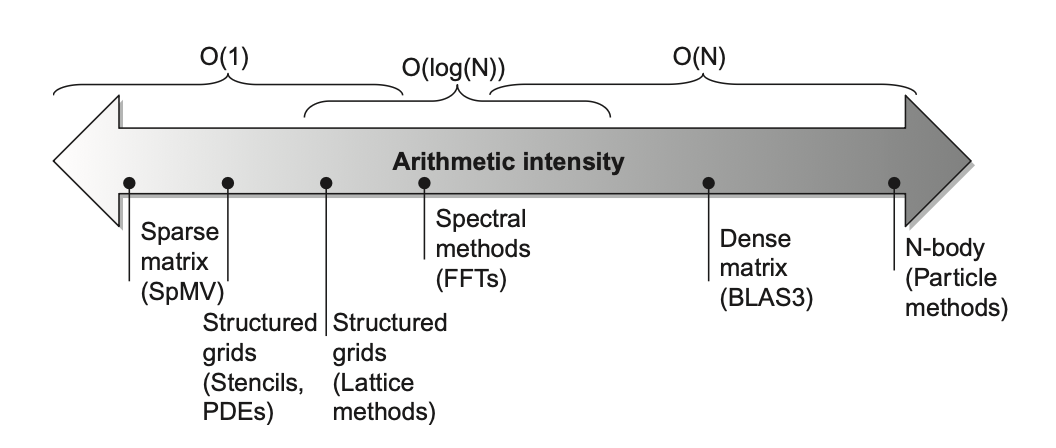
Peak floating-point performance can be determined by hardware specifications.
Many kernels in this case study cannot fit into the on-chip cache, so peak memory performance is defined by the memory system behind the cache, which can be obtained by running the Stream benchmark.
The following figure compares the performance of two processors using the roofline model:
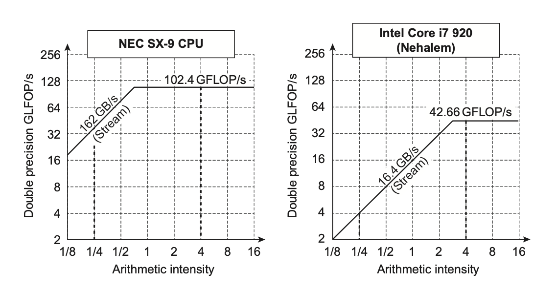
We can use the following formula to describe the curve in the roofline model:
Consider the convergence point of the diagonal and horizontal lines in the model:
If it is located far to the right, only a few kernels with high arithmetic intensity can achieve the computer’s maximum performance.
If it is located far to the left, almost all kernels can achieve maximum performance.
Compared to other SIMD processors, vector processors have both higher memory bandwidth and a convergence point that is further to the left.
4.3 Detecting and Enhancing Loop- Level Parallelism
The analysis of loop-level parallelism focuses on whether data accesses in subsequent iterations depend on data values produced in previous iterations. Such dependencies are called loop-carried dependencies.
Because finding loop-level parallelism involves identifying structures such as loops, array references, and induction variable computations, compilers can perform this analysis more easily at (or near) the source level than at the machine code level.
Our analysis must begin by identifying all loop-carried dependencies. This dependency information is inexact, in the sense that it tells us that such a dependency may exist.
Typically, data dependency analysis can only determine that one reference may depend on another; determining that two references must point to exactly the same address requires more complex analysis.
Loop-carried dependencies often form recurrences. A recurrence occurs when the definition of a variable is based on the value of that variable from a previous iteration (usually the immediately preceding one).
Finding Dependences
Obviously, identifying dependencies in a program is crucial for determining which loops may contain parallelism and for eliminating name dependencies. The complexity of dependence analysis also arises from the presence of arrays and pointers in languages like C/C++, or the pass-by-reference parameter mechanism in Fortran. Since scalar variables explicitly reference a name, analysis is usually relatively straightforward; however, pointers and reference parameters lead to aliasing issues, introducing complexity and uncertainty into the analysis.
Almost all compiler dependence analysis algorithms are based on the assumption that “array indices are affine.” In short, a one-dimensional array index is called affine if it can be expressed in the form a * i + b (where a and b are constants, and i is the loop index variable). For multi-dimensional arrays, if each dimension’s index is affine, then the multi-dimensional index is also affine. A typical example of non-affine access is sparse array access like x[y[i]].
Therefore, determining whether two accesses to the same array within the same loop have a dependence is equivalent to determining whether two affine functions can yield the same result at different index values within the loop bounds. For example: Suppose we store an array element with index value a * i + b, and later load data from the same array with index value c * i + d (where i is the for-loop variable, incrementing from m to n). A dependence exists when the following two conditions are met:
There are two iteration indices, j and k, both within the bounds of the for loop, i.e., m <= j <= n, m <= k <= n
The loop stores data to the array element indexed by a * j + b, and later retrieves it from the same array element when indexed by c * k + d, i.e., a * j + b == c * k + d
In general, we cannot determine at compile time whether a dependence exists. For example, the specific values of variables a, b, c, and d may be unknown (they could be elements from other arrays), making it impossible to determine whether a dependence holds. Additionally, dependence testing can be computationally expensive but still decidable at compile time, such as when access operations depend on the iteration indices of multiple nested loops. However, in most programs, subscript expressions are usually simple, with a, b, c, and d being constants. For such cases, reasonable compile-time dependence detection methods can be designed.
One simple and sufficient detection method is the Greatest Common Divisor (GCD) test, which can prove the absence of dependence. Its principle is based on the observation: if a loop-carried dependence exists, then GCD(c, a) must divide (d - b). In general, the GCD test is sufficient to guarantee that no dependence exists. However, there are cases where the GCD test passes, but no actual dependence exists. This occurs because the GCD test does not consider loop bounds.
In general, determining whether a dependence truly exists is an NP-complete problem. However, in practice, many common cases can be analyzed precisely at low cost. Recent research suggests that a hierarchical approach using a series of exact tests with increasing generality and cost can ensure both accuracy and efficiency. (An exact test refers to a method that can precisely determine whether a dependence exists.)
Beyond detecting the existence of dependencies, the compiler also needs to classify dependency types. This classification allows the compiler to identify name dependencies and eliminate them at compile time through renaming and copying.
For detecting loop-level parallelism, dependence analysis is the most fundamental tool. Whether compiling programs efficiently for vector computers, SIMD computers, or multiprocessor systems, this analysis is crucial. The main limitation of dependence analysis is that it only applies to specific scenarios—array access operations with affine index functions within a single loop nest. Therefore, there are many cases where array-oriented dependence analysis cannot provide the necessary information. For example, analyzing pointer access behavior is much more difficult than analyzing array indices (which is one reason why many scientific applications targeting parallel computing still prefer Fortran over C/C++). Similarly, analyzing references across procedure calls is extremely challenging. Thus, while analyzing code written in serial languages remains important, we also need programming models like OpenMP and CUDA that support explicit parallel loop programming.
Eliminating Dependent Computations
Earlier, we mentioned that one of the most important forms of dependent computation is recurrence, and the dot product is a good example:
for (i = 9999; i >= 0; --i) |
This loop cannot be parallelized because there is a loop-carried dependency on sum. However, we can transform this loop into a set of loops, where one loop within the set can be fully parallelized, while the remaining loops can only be partially parallelized. The fully parallelizable loop looks like this:
for (i = 9999; i >= 0; --i) |
Notice that the summation has been expanded from a scalar to a vector (this transformation is called scalar expansion), and this transformation allows the new loop to be fully parallelized. However, after completing this operation, we need to perform a reduction step, which sums the elements of the vector, as shown below:
for (i = 9999; i >= 0; --i) |
Although this loop is not a parallel structure, it has a special structure known as reduction. In vector and SIMD architectures, dedicated hardware is sometimes used to accelerate reduction operations, making the reduction step much faster than scalar mode. The implementation principle is similar to the technical approach used in multi-processor environments. While the general transformation applies to any number of processors, for simplicity, let’s assume we have 10 processors. In the first step of the summation reduction, each processor performs the following operation (where p represents the processor number from 0 to 9):
for (i = 999; i >= 0; --i) |
This loop, where each of the 10 processors accumulates 1000 elements, is fully parallelizable. Then, a simple scalar loop can aggregate the final 10 partial sums.
It is important to note: the aforementioned transformation relies on the associative property of addition. While mathematical operations satisfy associativity over infinite range and precision, computer arithmetic does not—integer operations are limited by finite numerical ranges, and floating-point operations are constrained by both range and precision. Therefore, using such restructuring techniques can occasionally lead to incorrect results (though the probability is extremely low). For this reason, most compilers require explicitly enabling optimizations that rely on associativity.
4.4 Cross-Cutting Issues
Energy and DLP
Assuming sufficient DLP, if we halve the clock frequency and double the execution resources, the processor’s performance remains unchanged. If we can simultaneously lower the voltage while reducing the clock frequency, we can actually reduce the energy consumption and power required for computation while maintaining peak performance. Therefore, GPUs often operate at lower clock frequencies than system processors, which rely on high clock speeds to improve performance.
Compared to out-of-order execution processors, DLP processors have simpler control logic and can issue a large number of operations per clock cycle: for example, the control signals for all lanes in a vector processor are completely identical, eliminating the need for logic circuits that determine multi-instruction issue or speculative execution. They also significantly reduce the workload of instruction fetching and decoding. Additionally, vector architectures can more easily shut down unused portions of the chip—each vector instruction explicitly declares all hardware resources it will occupy in the upcoming cycles at the time of issuance.
Banked Memory and Graphics Memory
The vector architecture requires sufficient memory bandwidth to support unit stride, non-unit stride, and gather-scatter access patterns. To achieve the highest memory performance, high-end GPUs from AMD and NVIDIA use stacked DRAM technology (also known as High Bandwidth Memory, or HBM), which packages memory chips and processing chips together in the same module. The ultra-wide data bus provides high bandwidth, while the co-packaging of memory and processing chips reduces latency and power consumption.
Considering all potential memory demands from computational tasks and graphics acceleration tasks, the memory system may encounter a large number of unrelated requests, which can degrade memory performance. To address this, the GPU’s memory controller maintains traffic queues for different memory partitions until sufficient traffic accumulates, at which point it opens a row and transfers all requested data at once. This delay improves bandwidth but increases latency, so the controller must ensure that no processing unit “starves” while waiting for data; otherwise, adjacent processing units may become idle.
Strided Accesses and TLB Misses
The interaction between the TLB of virtual memory in vector architectures or GPUs and strided access is a problem. Depending on the organization of the TLB and the size of the array being accessed in memory, it is possible that every access to an element in the array results in a TLB miss. The same type of conflict can also occur in the cache, but the performance impact may be smaller.
Chapter 5 Thread-Level Parallelism
5.1 Introduction
This chapter primarily explores thread-level parallelism (TLP). TLP utilizes MIMD (multiple instructions, multiple data).
As mentioned earlier, due to the slowdown in ILP technological advancements, the development of uniprocessors is gradually coming to an end. Consequently, the importance of multiprocessors is increasing—they consist of a set of tightly coupled processors controlled by the operating system, sharing memory through a common address space (not necessarily a single physical memory). Multiprocessors achieve TLP through two different software models:
- Parallel processing: A set of tightly coupled threads collaborating on a single task.
- Request-level parallelism: Execution of multiple relatively independent processes from one or more users. A single application running on multiple processors can utilize request-level parallelism, such as a database responding to queries, or through multiple independently running applications (the latter often referred to as multiprogramming).
Multiprocessors include both single-chip systems with multiple cores, known as multicore, and computers composed of multiple chips, where each chip is typically a multicore unit.
Later, we will also discuss multithreading—a technique that supports interleaved execution of multiple threads on a single multiple-issue processor. Many multicore processors also include support for multithreading.
Multiprocessor Architecture
To fully utilize an MIMD multiprocessor with n processors, at least n threads or processes are typically required for execution. Independent threads within a single process are usually explicitly specified by the programmer or dynamically created by the operating system based on multiple independent requests. At the other extreme, a thread may consist of only a few dozen iterations of a loop—generated by a parallel compiler exploiting data parallelism within the loop.
Although the amount of computation assigned to a thread (referred to as grain size) is crucial for efficiently exploiting TLP, the fundamental difference from ILP lies in the fact that TLP is identified by software systems or programmers at a high level of abstraction, consisting of code segments ranging from hundreds to millions of instructions that can be executed in parallel.
Threads can also be utilized for DLP, but their overhead is typically higher than that of SIMD processors or GPUs. It is essential to ensure that the grain size is large enough to efficiently exploit parallelism.
For existing shared-memory multiprocessors, they can be divided into two main categories based on their memory organization:
Symmetric (shared-memory) multiprocessors (SMP) (or centralized shared-memory multiprocessors)
Feature a small to moderate number of cores, typically 32 or fewer
In such multiprocessors with a limited number of cores, these processors can share a single centralized memory that all processors have equal access to, hence the term “symmetric”
Most current multicore processors fall under SMP
SMP is sometimes referred to as uniform memory access (UMA) multiprocessors. All processors uniformly share physical memory, with equal access time to any memory word, and each processor may have private caches or private memory.
Some multicore processors have non-uniform access to the outermost cache, a structure known as nonuniform cache access (NUCA), so even with a single main memory, they are not true SMPs
Distributed shared memory (DSM)
In multiprocessor systems composed of multiple multicore chips, each multicore chip typically has its own memory unit, so the memory in such systems is organized in a distributed rather than centralized manner
Many distributed memory designs enable fast access to local memory, while remote memory access is significantly slower
In such architectures, programmers and software systems must explicitly distinguish between local and remote memory access operations, but typically do not need to focus on the specific distribution among remote storage nodes
To support a larger number of processors, memory must be organized in a distributed rather than centralized fashion; otherwise, the memory system would need to meet the bandwidth demands of more processors at the cost of increased access latency
Due to these issues, SMP gradually loses its advantages as the number of processors increases, so the vast majority of large-scale multiprocessor systems adopt distributed memory organization
DSM multiprocessors are also known as nonuniform memory access (NUMA) architectures because data access time depends on the physical location of the data word in memory. All CPUs share a unified address space, using load and store instructions to access remote memory, which is slower than accessing local memory, and processors in NUMA systems can use caches.
The main disadvantage of DSM is that the data communication mechanism between processors becomes more complex, and more effort is required at the software level to fully leverage the advantages of increased memory bandwidth.
NUMA can be further divided into:
NC-NUMA: No cache, thus unable to hide the time required to access remote memory
CC-NUMA: Has a coherent cache
In both SMP and DSM architectures, communication between threads is achieved through a shared address space. This means that as long as the appropriate access permissions are in place, any processor can address any memory location. The shared memory in SMP and DSM essentially refers to the sharing of the address space.
Challenges of Parallel Processing
Multiprocessors have a wide range of applications, including:
Running independent tasks that require almost no communication
Or executing parallel programs that require inter-thread collaboration to complete
To address the challenges posed by these tasks, a comprehensive approach is typically required:
Carefully selecting algorithms and optimizing implementations
Adapting to the underlying programming language and system
Coordinating the operating system and its support functions
Adjusting the architecture and hardware implementation
Although one of these aspects may often become the primary bottleneck, when the processor scale becomes very large, we need to synchronously optimize all layers of software and hardware. Specifically, we mainly encounter the following two challenges:
Limited parallelism in programs (corresponding to the first application above)
Relatively high communication overhead, or the high latency of remote access in parallel processors (corresponding to the second application above). The specific duration depends on the communication mechanism, the type of interconnection network, and the scale of the multiprocessor
Both of the above issues can be explained by Amdahl’s Law.
The corresponding solutions are:
For the issue of insufficient application parallelism, the focus should be on the software level: on one hand, adopting new algorithms that provide better parallel performance; on the other hand, relying on the software system to maximize the effective execution time of the processor in its full configuration
To mitigate the impact of high remote latency, collaboration between architects and programmers is required: for example, reducing the number of remote accesses through hardware mechanisms (such as caching shared data) or software methods (such as restructuring data structures to localize access); or attempting to mask latency using multithreading techniques or prefetching strategies
5.2 Centralized Shared-Memory Architectures
Using large, multi-level caches can significantly reduce a processor’s demand for memory bandwidth, a discovery that has driven the development of centralized shared-memory multiprocessors.
Early processors were all single-core designs, typically occupying an entire motherboard, with memory located on a shared bus.
With the advent of high-performance processors, the memory demands of processors exceeded the capacity of conventional buses. As a result, modern microprocessors connect memory directly to a single chip—sometimes referred to as a backside bus or memory bus, to distinguish it from the bus used for I/O.
Whether performing I/O operations or handling accesses from other chips, accessing a chip’s local memory must go through the chip that “owns” that memory.
Therefore, this type of memory access is asymmetric: local memory access is fast, while remote memory access is slower.
In multi-core architectures, all cores on a single chip share that memory, but asymmetric access patterns often exist between different cores through their respective memories.
Symmetric shared-memory machines typically support caching of both private and shared data, where:
Private data is used by only one processor. When private data is cached, its storage location migrates to the cache, reducing average access time and memory bandwidth requirements.
Shared data can be accessed by multiple processors. When caching shared data, its value may be replicated across multiple caches. In addition to reducing access latency and memory bandwidth demands, this replication can alleviate contention issues that arise when multiple processors simultaneously read the same shared data item. However, caching shared data also introduces a new challenge—cache coherence.
Multiprocessor Cache Coherence
Cache Coherence Problem: This issue arises because two different processors build their views of memory through their respective caches, so these processors may ultimately see different values for the same memory location. The problem stems from the coexistence of a global state defined by main memory and local states defined by independent caches private to each processor core.
An informal way to put it is: if a memory system returns the most recently written value for any data item when it is read, we can say the memory system is coherent. While intuitive and easy to understand, this definition is vague and overly simplistic—the actual situation is far more complex. Moreover, this simple definition actually encompasses two aspects of memory system behavior:
Coherence: Specifies which values a read operation can return.
Consistency: Determines when the value of a write operation can be returned by a read operation.
A strict definition of coherence is: a memory system is said to be coherent when the following conditions are met:
A write by processor P to location X, followed immediately by a read by P from X, with no other processor writing to X between the write and the read, always returns the value written by P. This property preserves program order and holds even in a single processor.
When a read by a processor from location X occurs after a write by another processor to X, provided there is sufficient time between the read and write and no other write to X occurs between the two accesses, the read returns the written value. This property defines the core meaning of memory coherence: if a processor can consistently read stale data, the memory is clearly in an inconsistent state.
Write serialization: Writes to the same location are serialized. That is, any two writes to the same location by two processors are seen in the same order by all processors. For example, if values 1 and 2 are written sequentially to a location, no processor can read 2 before 1.
Although these three properties are sufficient to ensure coherence, consistency is equally crucial. For instance, we cannot require that a read from X immediately obtain the (latest) value written to X by another processor, because the written data may not have even left the original processor yet. Consistency is defined by the memory consistency model, which will be discussed later.
Coherence and consistency complement each other:
Coherence governs the behavior of read and write operations to the same memory address.
Consistency defines the behavior of read and write operations involving different memory addresses.
For now, we make the following two basic assumptions:
A write operation is not considered complete (and subsequent writes are not allowed to proceed) until all processors are aware of its result.
A processor must not reorder any write operation relative to other memory accesses. This means that if a processor writes to address A and then to address B, any processor that observes the new value of B must also have obtained the new value of A.
These assumptions allow processors to reorder read operations but force them to complete writes in program order. These assumptions will remain in effect until the introduction of the “memory consistency model.”
Basic Schemes for Enforcing Coherence
In programs running on multiprocessors, multiple copies of the same data often exist simultaneously in various levels of cache. In a coherent multiprocessor, the cache provides both migration and replication of shared data.
Migration: Data items can be transparently moved to the local cache and used. This reduces both the latency of accessing remotely allocated shared data and the bandwidth pressure on the shared memory.
Replication: Effectively reduces access latency and resource contention when reading shared data.
Thus, achieving efficient migration and replication is crucial for improving the performance of shared data access. Therefore, multiprocessors introduce hardware-level protocols to maintain cache coherence. These protocols are called cache coherence protocols, and their core implementation lies in tracking the sharing state of data blocks. The state of each cache block is maintained through associated status bits (similar to the valid and dirty bits in a uniprocessor cache). Based on different implementation techniques, these protocols can be divided into two categories:
Directory-based:
The sharing state of a specific physical memory block (which processor has a copy of a particular memory block in its cache) is stored in a location called the directory.
There are two distinct directory-based cache coherence schemes:
In SMP, a centralized directory associated with memory or another single serialization point (such as the outermost cache of a multi-core chip) can be used.
In DSM, since a single directory hinders performance and struggles to meet the memory scaling requirements of multi-core architectures, a distributed directory is required, though it is more complex to implement.
Snooping:
Each cache holding a copy of a physical memory block can track the sharing state of that block.
In SMP, the caches of individual cores typically communicate via a broadcast medium (such as the bus between the core’s own cache and the shared cache/memory), and all cache controllers continuously monitor or snoop the medium to determine if they have a copy of the requested data block on the bus or in exchange access.
Snooping techniques are also applicable to coherence protocols in multi-chip multiprocessors.
Snooping protocols are widely popular in multiprocessor systems that use microprocessors (single-core) connected to a single shared memory via a bus. The bus provides a convenient broadcast medium for implementing snooping protocols. However, multi-core architectures have changed this landscape, as all cores on a multi-core chip share a certain level of cache. Consequently, some designs have shifted to directory protocols due to their lower overhead.
We will first focus on snooping protocols and discuss directory protocols in detail when we cover DSM architectures.
Snooping Coherence Protocols
To maintain cache coherence, there are two methods:
Write Invalidate Protocol: Ensures that a processor has exclusive access to a data item before writing to it.
- Exclusive access guarantees that when a write operation is performed on a shared cache line, all copies of that cache line in other caches are invalidated.
- When other processors subsequently read the data, a cache miss occurs, requiring them to fetch the updated data from memory or from a cache holding a valid copy (resulting in longer read latency). This reduces bandwidth consumption caused by repeated writes on the bus.
- If two processors attempt to write to the same data simultaneously, one will succeed, causing the other’s data copy to be invalidated. The other processor must obtain a new copy of the data containing the latest updated value to complete its write operation.
- Thus, this protocol ensures write serialization.
- This is currently the most mainstream protocol.
Write Update / Write Broadcast Protocol: Whenever a processor writes to a shared cache line, it broadcasts the new value to update all copies of that cache line in other caches.
- Since the write update protocol must broadcast write operations to all shared cache lines, it consumes more bandwidth.
Therefore, almost all modern multiprocessor systems choose to implement the write invalidate protocol, and we will focus only on this protocol moving forward.
Basic Implementation Techniques
We also need to locate data items when a cache miss occurs:
In a write-through cache, finding the current value of a data item is relatively simple because all written data is immediately sent to memory, where the latest value of the data item can always be obtained.
Summary: Various scenarios of read/write operations in a snooping cache
For a write-back cache, determining the latest data value is more difficult because the latest value of a data item may exist in a private cache rather than in a shared cache or main memory.
However, we can apply the same snooping mechanism to cache misses and write operations: each processor snoops on all addresses transmitted on the shared bus; when a processor finds that it holds a dirty copy of the target cache block, it returns that cache block as the response to the read request and terminates the access to main memory (or the L3 cache). The complexity of this method lies in the need to obtain the target block from another processor’s private cache (L1 or L2), which typically takes longer than accessing the L3 cache.
Since write-back caches have lower memory bandwidth requirements, they can support the collaboration of more high-speed processors. For this reason, all multi-core processors adopt a write-back strategy in the outermost cache.
Next, we will explore consistency implementation schemes based on write-back caches.
The conventional cache tags can be used to implement the snooping mechanism, and the valid bit of each block makes invalidation operations easy to implement.
Handling read misses triggered by invalidation or other events is also straightforward, as they rely solely on the snooping function.
For write operations, we need to know whether there are other cached copies of the block. If not, in a write-back cache, there is no need to place this write operation on the bus. Not sending a write request reduces write time and saves bandwidth.
To track whether a cache block is shared, we can add an additional state bit for each cache block, enabling us to determine whether a write operation needs to generate an invalidation signal.
When writing to a block in a shared state, the cache generates an invalidation command on the bus and marks the block as exclusive. After that, the core no longer sends any invalidation requests for this block.
The core holding the only copy of a cache block is typically referred to as the owner of that cache block.
When an invalidation instruction is sent, the owner’s cache block state changes from shared to non-shared (or exclusive). If another processor later requests this cache block, its state must be set back to shared.
Since our snooping cache can also detect any invalidation, it can know when an exclusive cache block is requested by another processor and restore the state to shared.
Each bus transaction must check the cache address tags, which may interfere with the processor’s cache access. To reduce this interference, we have the following measures:
Duplicate the tags and direct snooping accesses to the tag copies.
Use a directory at the shared L3 cache. This directory can indicate whether a given block is shared and which cores may have copies. With directory information, invalidation operations can target only those caches that hold copies of the cache block. This requires that the L3 always retain copies of any data items in L1 or L2, a property known as inclusion.
A Simple Protocol
We generally implement a snooping coherence protocol by integrating a finite state controller into each core. This controller responds to requests from the in-core processor and the bus (or other broadcast medium), changing the state of selected cache blocks while using the bus to access data or invalidate it. Logically, each cache block can be considered to have its own independent controller, meaning that snooping operations or cache requests for different cache blocks can be processed independently. In practice, a single controller allows multiple operations on different cache blocks to be executed in an interleaved manner.
We define the protocol to include three states:
Invalid: The data in the cache line is invalid.
Shared: Indicates that the block in the private cache may be shared by multiple cores.
Modified: Indicates that the block has been updated in the private cache; this state also implies that the block is exclusive. At this point, the corresponding data in memory and any copies of the data in other caches are invalid (since they do not contain the most recent data).
When an invalidation request or write-invalidate appears on the bus, all cores that have a copy of the cache block in their private caches set it to invalid. In the case of a write-invalidate for a write-back cache, if the block exists only in one private cache and is in an exclusive state, that cache must also perform a write-back operation; otherwise, the data can be read directly from the shared cache or main memory.
The figure below shows the finite state transition diagram for a single private cache block using a write-invalidate protocol and a write-back cache (the left diagram shows CPU requests, and the right diagram shows bus requests):
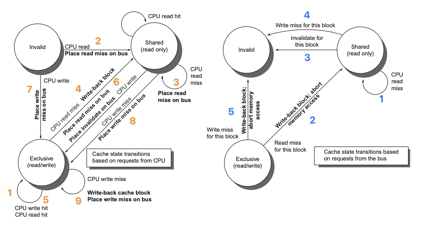
Merging the two state transition diagrams together yields the following state diagram:
Any valid cache block is either in a shared state across one or more private caches or strictly in an exclusive state within a single cache.
Any transition to the exclusive state (which is necessary for a processor to write to the block) requires an invalidate or write-invalidate signal on the bus, causing all local caches to set the block to an invalid state.
Additionally, if another local cache previously held the block in an exclusive state (making it dirty), that cache performs a write-back operation, providing the data block containing the target address.
Finally, when a read miss occurs on the bus for a block in the exclusive state, the local cache holding the exclusive copy changes its state to shared.
Another characteristic of this protocol is that a memory block in the shared state always remains up-to-date in the external shared cache (L2 or L3, or memory if no shared cache exists). This feature significantly simplifies the implementation.
Although this simple cache protocol executes correctly, it overlooks many complexities. Most importantly, it assumes that all operations are atomic—meaning each operation can complete without interference from others—which is not the case in reality. Non-atomic operations introduce the possibility of protocol deadlock, where the system enters a state from which it cannot proceed. We will discuss these scenarios later.
Extensions to the Basic Coherence Protols
The consistency protocol described earlier is a simple three-state protocol, commonly referred to by the initials of its states, hence known as the MSI (Modified, Shared, Invalid) protocol. We can extend this basic protocol by adding additional states and transactions to optimize specific behaviors, thereby (potentially) improving performance. Among the most common extensions are:
MESI protocol: Adds an exclusive state, resulting in four states: Modified, Exclusive, Shared, and Invalid.
The exclusive state indicates that the cache block exists only in a single cache and has not been modified.
If a block is in the exclusive state, writing to it does not require generating an invalidation signal, thus optimizing scenarios where the same cache first reads and then writes to the data block.
Of course, when a read miss occurs for a block in the exclusive state, the block must be transitioned to the shared state to maintain consistency.
The advantage of adding the exclusive state is that when the same core writes again to a data block in the exclusive state, it neither needs to acquire bus access nor generate an invalidation signal, because the system knows that the data block exists only in this local cache; the processor only needs to change its state to modified to complete the update.
This state extension can be easily implemented by encoding the consistency state bit as an exclusive state bit and using a dirty bit to indicate modification.
Below is the state diagram of the MESI protocol (jxh version):
MOESI protocol: Based on the MESI protocol, it adds an “owned” state, indicating that the relevant cache block is held by this cache and the copy in main memory is outdated.
In the MSI and MESI protocols, when attempting to share a cache block in the modified state, the state of the block in both the original cache and the new shared cache transitions to the shared state, and it must be written back to main memory.
In the MOESI protocol, the modified state of the original cache can directly transition to the owned state without immediately writing to memory. Other new caches sharing the block remain in the shared state; the owned state held only by the original cache indicates that the main memory copy is invalid and designates the cache as the owner.
When a miss occurs, the owner must provide the data block (since main memory is not updated); if it is evicted, it must be written back to main memory.
Limitations in SMPs and Snooping Protocols
As the number of processors in a multiprocessor system increases, or as the memory demand per processor grows, any centralized resource in the system can become a bottleneck. For multi-core processors, even a small number of cores can cause a single shared bus to become a performance bottleneck. Therefore, multi-core designs have shifted toward higher-bandwidth interconnection schemes and the use of multiple independent memories to support a larger number of cores.
The bandwidth of snooping caches can also be a limitation, as each cache must check every miss, and increasing interconnect bandwidth only shifts the problem to the caches. Below are some techniques to increase snooping bandwidth:
Replicating tag bits to double bandwidth.
If multi-core processors share the outermost cache, a distributed cache can be used—each processor manages a portion of the memory region and handles snoop requests for the corresponding address space.
- Since the L3 cache serves to filter snoop requests, it must be inclusive.
A directory can be set up at the outermost shared cache level (e.g., L3).
Similarly, the L3 cache must remain inclusive.
With the introduction of a directory structure, there is no need to broadcast to all L2 caches; instead, only the specific L2 caches that may hold copies of the data block, as indicated by the directory, need to be queried.
Similar to the previous method, the associated directory entries can also be stored in a distributed manner.
Implementing Snooping Cache Coherence
In a single-bus multi-core processor, the following methods can be used to make these steps substantially atomic:
First (before changing the cache state), arbitrate for the bus leading to the shared cache or memory, and do not release the bus until all operations are completed.
Use a single line to indicate that all necessary invalidation requests have been received and are being processed.
Upon receiving this signal, the processor that generated the invalidation signal can release the bus, knowing that all required operations will be completed before any activity related to the next invalidation is processed.
In a system without a single centralized bus, other methods are used to achieve atomicity of cache invalidation operations. Specifically, it must be ensured that when two processors attempt to write to the same data block simultaneously (a situation called a race), a strict order is followed: one write operation is fully processed and completed before the other write operation can begin execution. Which write operation wins the race is not important; the key is that there is only one winner, and its consistency operation completes first.
In a multi-core architecture using a multi-bus design, as long as each memory block is associated with only one independent bus, access requests to the same data block can be serialized through that shared bus, thereby eliminating race conditions. This feature, combined with the ability to restart the cache invalidation process for the losing party in a race, constitutes a key element of snooping-based cache coherence that can be implemented without a single bus.
In practical designs, a mix of snooping protocols and directory protocols can be used.
5.3 Distributed Shared-Memory and Directory-Based Coherence
The previously introduced snooping protocol requires communication with all other caches every time a cache invalidation occurs. This characteristic of not using a centralized data structure to track cache states is both an advantage of the snooping approach (low implementation cost) and its fatal weakness, as it results in poor scalability.
In recent years, the development of multi-core processors has forced all designers to adopt distributed memory to meet the bandwidth demands of each processor. This memory organization can improve memory bandwidth and interconnect bandwidth by separating local memory traffic from remote memory traffic, thereby reducing the bandwidth requirements on the memory system and interconnect network. However, if the broadcast operations required for cache invalidation in coherence protocols cannot be eliminated, the benefits of distributed memory will be extremely limited.
Additionally, we have mentioned an alternative to the snooping protocol—the directory protocol.
The directory records the state information of each potentially cached block, including which caches (or cache groups) hold copies of the block and whether the data is dirty (modified).
In multi-core processors with a shared last-level cache (L3), implementing the directory mechanism is very simple: it only requires maintaining a bit vector for each L3 cache block, with a length equal to the number of cores. This bit vector identifies which private L2 caches may hold a copy of the corresponding block in the L3 cache, so invalidation requests only need to be sent to these specific caches. When the L3 adopts an inclusive design, this mechanism works perfectly on a single multi-core chip.
In multi-core systems, a solution using a single directory is not scalable, even if it avoids broadcast operations. Therefore, we must set up distributed directories, but the distribution must ensure that the coherence protocol can locate the directory information for any cached memory block. An obvious solution is to distribute the directories along with the memory units—just as different memory requests point to different memory locations, different coherence requests can access different distributed directories. If the information is maintained in a partitioned last-level cache, such as the L3 cache, the directory information can be distributed across cache partitions, effectively improving bandwidth utilization.
Distributed directories have the following characteristic: the shared state of a block is always located at a single known location. This property, combined with information about the cache blocks held by nodes, allows the coherence protocol to avoid broadcast operations.
The simplest directory implementation associates an entry in the directory for each memory block. In this case, the total amount of information is proportional to the product of the number of memory blocks and the number of nodes. For multiprocessors with no more than a few hundred processors (each possibly multi-core), this overhead is acceptable with a reasonable block size.
For larger-scale multiprocessor systems, methods that efficiently scale the directory structure are needed, but we do not need to consider this scenario.
Directory-Based Cache Coherence Protocols
The directory protocol must implement two core operations: handling read misses and processing writes to shared and clean cache blocks.
To achieve these functions, the directory needs to track the state of each cache block. Specifically, the following states exist:
Shared: One or more nodes have cached the data block, and the value in memory remains synchronized with all cached copies.
Uncached: No node holds a copy of the cache block.
Modified: Only one node holds a copy of the data block and has performed a write operation, rendering the corresponding copy in memory invalid. In this case, the processor is referred to as the owner of the data block.
In addition to tracking states, it is also necessary to record which nodes have copies of the memory block, as these copies need to be invalidated during a write. The simplest way to implement this is to maintain a bit vector for each memory block. When the memory block is in the shared state, each bit in the vector indicates whether the corresponding processor chip holds a copy of the block. When the memory block is in the exclusive state, this bit vector can also be used to track its owner.
For efficiency, the state of each cache block is also recorded separately in the various levels of cache.
Although the specific operations during state transitions differ slightly, the state machine states and transition mechanisms in each cache are entirely consistent with the previously used snooping-based cache scheme.
However, there are significant differences in the invalidation of data items and the location of exclusive copies: both operations require communication between the requesting node and the directory, as well as between the directory and one or more remote nodes. In the snooping protocol, these two steps are accomplished by broadcasting to all nodes simultaneously.
The following diagram illustrates the various types of messages exchanged between nodes:
A local node is the node that initiates the request, while a home node is the node that stores the memory location and directory entry corresponding to the target address.
The physical address space adopts a static distribution scheme, so it is always possible to determine which node holds the memory and directory information for a specific physical address (e.g., high-order bits can represent the node number, while low-order bits indicate the offset within that node’s memory).
Even when the home node is also the local node, the directory must still be accessed because data copies may exist in a third-party node called a remote node.
A remote node is a node that holds a copy of a cache block (regardless of whether the copy is in an exclusive or shared state).
The remote node may be the same as the local node or the home node. In such cases, inter-processor messages can be replaced by intra-processor messages, while other mechanisms remain unchanged.
An Example Directory Protocol
The following diagram shows the state transition diagram of a single cache block in a directory-based system:
This state transition diagram is largely consistent with the snooping-based approach: the states and triggering conditions are nearly identical.
The difference is that in the snooping mechanism, write-invalidation operations are broadcast via a bus (or other network), whereas here, we use a directory controller to selectively send data fetch and invalidation operations.
Any cache block must be in an exclusive state when being written, and all shared blocks must maintain the latest value in memory.
In most multi-core processors, the outermost cache is shared by all cores, and an internal directory or snooping mechanism is used to maintain cache coherence among the private caches of each core on the same chip. Therefore, by simply connecting to the outermost shared cache, the on-chip multi-core coherence mechanism can be extended to larger processors. This also alleviates contention issues between processors and coherence requests while avoiding duplication of tag bits.
In directory-based protocols, messages sent to the directory trigger two different types of operations: updating the directory state and sending additional messages to satisfy the request. The state in the directory represents the three standard states of a memory block; however, unlike the snooping scheme, the directory state here reflects the overall status of all cache copies rather than the state of a single block.
To track the set of nodes holding copies of a cache block, we use a bit vector called Sharers. Directory requests need to update the sharers and perform invalidation operations by reading this set.
The following diagram shows the operations taken by the directory node upon receiving a message (the state diagram structure is consistent with the one above):
This directory handles three different types of requests: read miss, write miss, and data write-back.
To understand the mechanisms of these directory operations, we will analyze step by step the requests received and the operations performed in each state.
When a block is in the uncached state, the copy in memory is the current valid value, so the following types of requests may occur:
Read miss: The requesting node obtains the requested data from memory, and this requester becomes the only sharing node; at this point, the state of the data block is set to the shared state.
Write miss: The requesting node receives the value and becomes the sharing node; the data block is set to the exclusive state to indicate that its only valid copy is cached; the Sharers field identifies its owner.
When a block is in the shared state, the memory value is up to date, so the following requests may occur:
Read miss: The requested data is sent from memory to the requesting node, and the requesting node is added to the Sharers.
Write miss: The value is sent to the requesting node; invalidation messages are sent to all nodes in the Sharers, and the Sharers are updated to include only the identifier of the requesting node; at this point, the state of the block is set to the exclusive state.
When a block is in the exclusive state, the current value of the block is held in the cache of the node identified by the Sharers (owner), so the following directory requests exist:
Read miss: A data fetch message is sent to the owner, which transitions the state of the block in the owner’s cache to the shared state and prompts the owner to send the data to the directory. The data is written to memory at the directory and then sent back to the requesting processor. The identity of the requesting node is added to the Sharers, which still includes the identity of the original owner processor (since it still holds a readable copy).
Data write-back: Since the owner is replacing the block, it must be written back. This operation updates the memory copy to the latest state (the home directory essentially becomes the new owner), at which point the block transitions to the uncached state and the Sharers are cleared.
Write miss: The block will belong to a new owner. A message is sent to the original owner to invalidate the block in its cache and transfer the value to the directory; the directory then forwards the value to the requesting node, making it the new owner. The Sharers are updated to the information of the new owner, and the exclusive state of the block remains unchanged.
5.4 Synchronization
Why is synchronization needed? Because it is necessary to know when different processes can safely use shared data.
Synchronization mechanisms are typically built from user-level software routines that rely on hardware-provided synchronization instructions. For smaller-scale multiprocessor systems or low-contention scenarios, the key hardware capability is to provide an uninterruptible instruction or instruction sequence that can atomically retrieve and modify a value. Based on this capability, software synchronization mechanisms can be constructed. This section focuses on the implementation principles of two synchronization operations: locking and unlocking. Through these two operations, both mutual exclusion control can be achieved, and a foundation can be laid for more complex synchronization mechanisms.
Basic Hardware Primitives
In a multiprocessor system, the key capability required to implement synchronization is a set of hardware primitives that can atomically read and modify a memory location. Without this capability, the cost of building basic synchronization primitives would be extremely high and would increase with the number of processors. In fact, there are multiple alternative basic hardware primitives, all of which provide the ability to atomically read and write a location. However, architects generally do not expect users to directly use these basic hardware primitives; instead, they expect system programmers to use them to build synchronization libraries. Let us start with one of these hardware primitives and demonstrate how it can be used to construct some basic synchronization operations.
The hardware primitive we will introduce is atomic exchange, which swaps the value in a register with the value in memory.
Suppose we need to build a simple lock: 0 indicates the lock is free, and 1 indicates the lock is held.
A processor attempts to acquire the lock by executing an exchange instruction: it swaps a register containing 1; the register’s memory address corresponds to the lock. If another processor already holds the lock, the exchange instruction returns 1; otherwise, when it returns 0, the memory location’s value is simultaneously updated to 1, preventing other competing exchange operations from also obtaining 0.
For example, when two processors simultaneously attempt to execute an exchange instruction, this contention is resolved: one processor will inevitably complete the exchange first and return 0, while the second processor’s exchange will return 1.
The key to using the exchange primitive for synchronization lies in its atomicity: the entire exchange process is indivisible, and two concurrent exchanges are serialized through write serialization.
There are also other atomic primitives for synchronization, but they all share a key feature: they read and update a memory value in a way that allows determining whether two operations are executed atomically. Below are some of these atomic primitives:
Test-and-set: Tests a value and sets a new value if the test passes. We can define an operation that checks whether a value is 0 and sets it to 1, used similarly to the atomic exchange operation.
Fetch-and-increment: Returns the value of a memory location and atomically increments it. By using 0 to indicate that the synchronization variable is not held, we can use this instruction similarly to the exchange operation.
Implementing a single atomic memory operation presents challenges because it requires completing both a memory read and write within an uninterruptible instruction. This requirement complicates consistency implementation—hardware must not allow any other operation to be inserted between the read and write, and must also avoid deadlock situations.
Another type of hardware primitive uses a pair of instructions, where the return value of the second instruction indicates whether the pair was executed atomically. If the pair appears as though all other processors’ operations occurred either entirely before or after them, then the pair is effectively atomic. This is the approach adopted by the MIPS and RISC-V architectures.
In RISC-V, this pair includes a special load operation (called load reserved) lr and a special store operation (called store conditional) sc.
Load reserved loads the memory content specified by rs1 into the rd register and creates a reservation on that memory address.
Store conditional stores the value in rs2 to the memory address specified by rs1.
If another write operation invalidates the reservation on that memory location during this period, the store conditional fails and writes a non-zero value to rd.
If successful, it writes 0 to rd.
If a context switch occurs between the two instructions, the store conditional also fails.
We can use this pair to construct other synchronization primitives.
The reserved register tracks the address specified by the lr instruction.
If an interrupt occurs, or if the cache block corresponding to the address in the link register is invalidated (e.g., by another sc instruction), the link register is cleared.
The sc instruction only checks whether its address matches the reserved register’s address: if it matches, it succeeds; otherwise, it fails.
Since the store conditional will fail after any repeated store attempt to the load reserved address or any exception, the instructions inserted between these two must be chosen carefully. Therefore, only register-to-register operations should be safely allowed; otherwise, deadlock may occur.
Additionally, to reduce the probability of store conditional failures caused by unrelated events or competing processors, the number of instructions between load reserved and store conditional should be kept as small as possible.
Implementing Locks Using Coherence
Once atomic operations are available, the consistency mechanism of multiprocessors can be used to implement spin locks. The processor continuously attempts to acquire such locks, looping until successful. Programmers use spin locks when they expect the lock to be held for a short time and want the locking process to have low latency when the lock becomes available. However, spin locks cause the processor to occupy resources while looping in a waiting state, making them unsuitable in certain scenarios.
Without a cache coherence mechanism, the simplest implementation is to store the lock in memory.
The processor can continuously attempt to acquire the lock through atomic operations and check whether the swap operation returns a lock in an idle state.
When releasing the lock, the processor only needs to store the value 0 at that address to unlock it.
The code sequence for a spin lock is as follows:
addi x2,R0,#1 |
If a multiprocessor supports cache coherence, locks can be cached through this mechanism to maintain lock consistency. A caching lock has the following advantages:
It allows the “spinning” process (i.e., repeatedly testing and acquiring the lock in a tight loop) to be performed on a local cached copy, without needing to access global memory each time an attempt is made to acquire the lock.
The previous spin lock process needs to be modified so that it spins by performing read operations on the local copy of the lock until it successfully sees that the lock is available.
The process attempts to acquire the lock by performing a swap operation; the processor first reads the lock to test its state.
The processor continues reading and testing until the read value indicates that the lock is unlocked.
The processor then competes with all other similarly “spinning” processes to see which one can lock the variable first.
All processes use a swap instruction: this instruction reads the old value and stores 1 into the lock variable; the sole winner sees 0, while the losers see the 1 placed by the winner.
The winning processor executes the code following the lock, and upon completion, stores 0 into the lock variable to release the lock, then a new competition begins.
The following is the code for executing this spin lock (note: 0 indicates unlocked, 1 indicates locked):
lockit: ld x2,0(x1) ; load of lock |
- The processor that recently used the lock is likely to use it again in the short term. At this point, the lock may still remain in the processor’s cache, significantly reducing the time required to acquire the lock.
The following table illustrates the interaction between the processor and the bus/directory when multiple processes compete to lock a variable using atomic exchange instructions:
When the processor holding the lock writes 0 to the lock, all copies in other caches are invalidated and must fetch the new value to update their local copies.
One of the caches will be the first to obtain the unlocked state value (0) and successfully acquire the lock through an exchange operation. Then, when the cache invalidation requests from other processors receive a response, they will find that the variable is already locked, so they can only continue testing and remain in a spinning state.
Barrier Synchronization
Barrier forces processes to wait until all processes have reached the barrier before releasing them to continue execution. Its implementation is mainly based on:
- Shared counter
- Spin waiting to release signals
Below is a piece of code related to the implementation of a barrier:
{ |
This code has a problem: in the barrier, the slower processes may be trapped by the fastest process. Therefore, the following improvements have been made:
Counting after leaving the barrier: Use an additional shared counter to count the processes in the barrier. Prevent any process from re-entering the barrier before all processes have left the previous instance. However, this method introduces additional latency and is therefore not recommended.
Sense-reversing barrier: This method solves the problem of processes being trapped, but the performance is still not high. The implementation code is as follows:
{ |
To improve barrier performance, we can adopt a software optimization—the combining tree barrier: using a predetermined n-ary tree structure, processes synchronize at child nodes and then report to the parent node, until the root node releases all processes. This reduces contention at a single synchronization point.
5.5 Models of Memory Consistency
Determining the degree of memory consistency is a rather complex issue.
The most intuitive model of memory consistency is called sequential consistency. It requires that the result of any execution is the same as if the memory access operations issued by each processor maintain their program order, and the access operations between different processors can be interleaved arbitrarily. This model eliminates the possibility of certain non-intuitive executions in the previous example, because all assignment operations must be completed before the IF statement begins execution.
The simplest way to achieve sequential consistency is to require the processor to delay the completion of any memory access until all invalidation operations triggered by that access are finished. Of course, an equally effective method is to delay the next memory access until the previous one is completed. It is important to remember that memory consistency involves operations on different variables: the two accesses that must be executed in order actually target different memory locations. In the example above, the reading of A or B (A == 0 or B == 0) must be delayed until the previous write operation (B = 1 or A = 1) is completed. Under the sequential consistency model, a write operation cannot simply be placed in the write buffer and then immediately followed by a read.
Although sequential consistency provides a simple programming paradigm, it can reduce potential performance, especially in multi-core systems with a large number of processors and high interconnect latency.
To achieve better performance, there are two approaches:
Retain sequential consistency but use latency-hiding techniques.
Use a memory consistency model with fewer restrictions that allows hardware to accelerate execution. This may change the programmer’s perception of multiprocessors, so before exploring these relaxed models, we need to understand the programmer’s expected needs.
The Programmer’s View
Although the sequential consistency model has performance disadvantages, from a programmer’s perspective, it offers the advantage of simplicity. We hope to develop a programming model that is both easy to explain and allows for high-performance implementation.
One programming model that achieves efficient execution assumes that programs are synchronized.
- A program is considered synchronized if all accesses to shared data are ordered through synchronization operations.
- A data reference is said to be ordered by synchronization operations if and only if, in all possible executions, a write operation by one processor to a variable and an access (read or write) by another processor to the same variable are separated by a pair of synchronization operations—the first performed by the writing processor after the write, and the second by the accessing processor before the access.
- A situation where a variable may be updated without being ordered by synchronization is called a data race, because the execution result depends on the relative speeds of the processors; similar to races in hardware design, the outcome is unpredictable. This also gives synchronized programs another name: data-race-free.
It is widely believed that most programs are synchronizable. This is because if accesses are not handled through synchronization, the program’s behavior becomes unpredictable—differences in execution speed determine which processor wins the data race, thereby affecting the final program result. Even under sequential consistency, reasoning about such programs is extremely difficult.
Programmers could attempt to ensure sequentiality by constructing their own synchronization mechanisms, but this is extremely complex, error-prone, and may lack architectural support—meaning these mechanisms could fail in future multiprocessor iterations. Therefore, the vast majority of programmers choose to use proven synchronization libraries optimized for multiprocessors and synchronization types.
Additionally, using standard synchronization primitives ensures that even if the underlying architecture implements a memory consistency model more relaxed than sequential consistency, correctly synchronized programs will behave as if the hardware implements sequential consistency.
Relaxed Consistency Models
The core idea of the relaxed consistency model is to allow read and write operations to complete out of order, but enforce ordering through synchronization operations, so that the behavior of synchronized programs appears as if the processor has sequential consistency. Depending on which read-write orders are relaxed, there are various classifications of relaxed consistency models. We define ordering relationships using a set of rules in the form of X -> Y, indicating that operation X must complete before operation Y begins. Sequential consistency requires maintaining all four possible orders: R -> W, R -> R, W -> R, W -> W. Relaxed models are defined by relaxing subsets of these four orders:
Relaxing only the W -> R order results in a model known as total store ordering or processor consistency. Since this model preserves the order of write operations, many programs that follow sequential consistency can adopt this model without additional synchronization operations.
Relaxing both W -> R and W -> W orders results in a model known as partial store order.
Relaxing all four orders leads to a series of models, including weak ordering, the PowerPC consistency model, release consistency, and the RISC-V consistency model.
By relaxing these ordering constraints, processors can achieve significant performance advantages, which is why RISC-V, ARMv8, and the C++/C language standards have chosen relaxed consistency as their memory model.
Release consistency distinguishes between two types of synchronization operations:
Acquire operations (marked as ) used to gain access to shared variables.
Release operations (marked as ) used to release objects to allow other processors to gain access.
In synchronized programs, acquire operations must precede the use of shared data, while release operations must occur after all updates to shared data and before the next acquire operation. This characteristic allows us to moderately relax ordering requirements—ensuring that read and write operations occurring before an acquire do not need to complete before that acquire, and read and write operations occurring after a release do not need to wait for that release to complete.
The following diagram illustrates the ordering constraints of various consistency models for general accesses and synchronization accesses:
Releasing coherence provides one of the most relaxed and easily verifiable models, ensuring that synchronization programs observe sequentially consistent execution results. Although most synchronization operations are either acquire or release, some operations combine both acquire and release semantics, resulting in ordering effects equivalent to weak ordering. While synchronization operations always guarantee that previous write operations have completed, we sometimes need to ensure the completion of write operations without relying on specific synchronization operations. In such cases, an explicit instruction—called FENCE in RISC-V—is required to ensure that all previous instructions in the thread have completed execution, including all memory writes and the completion of related invalidation operations.
5.6 Cross-Cutting Issues
Since multiprocessors redefine many system characteristics (such as the importance of performance evaluation, memory latency, and scalability), they introduce design issues that span the entire technology domain, affecting both hardware and software. This section will provide several examples centered around the problem of memory coherence.
Compiler Optimization and the Consistency Model
Another reason for defining a memory consistency model is to clarify the scope of legal compiler optimizations on shared data.
In explicitly parallel programs, unless synchronization points are clearly defined and the program is synchronized, the compiler cannot swap read and write operations on two different shared data items, as such transformations may affect program semantics. This restriction even hinders relatively simple optimizations (such as register allocation for shared data), as this process typically involves swapping reads and writes.
In implicitly parallelized programs (such as code written in High Performance Fortran (HPF)), this issue does not arise because the program must be synchronized and synchronization points are known.
From both research and practical perspectives, whether a more relaxed coherence model can bring significant advantages to compilers remains an open question, and the lack of a unified model is likely to delay the deployment of compilers.
Using Speculation to Hide Latency in Strict Consistency Model
The speculation techniques discussed in Chapter 3 can be used to hide memory latency. They can also be employed to mask the latency caused by strict coherence models, thereby gaining the advantages of a relaxed memory model. The core idea is that the processor dynamically reorders memory accesses through out-of-order execution, allowing instructions to execute in a non-sequential order. This out-of-order memory access may violate the principle of sequential consistency, thereby affecting program execution results. This issue can be avoided by leveraging the delayed commit feature of processors that support speculative execution: assuming the cache coherence protocol operates based on an invalidation mechanism, if the processor receives an invalidation notification for a memory address before the corresponding memory reference operation is committed, it triggers a speculative recovery mechanism to roll back the computation and restart execution from the invalidated memory reference.
If the processor’s reordering of memory requests leads to an execution order that could produce results different from those seen under sequential consistency, the processor will re-execute. The key to this approach is that the processor only needs to ensure that the final result is the same as if all accesses were completed in order, by detecting situations where discrepancies might occur. The advantage of this scheme is that speculative restarts are rarely triggered, only when unsynchronized accesses actually cause a race condition.
Some argue that combining sequential or processor consistency with speculative execution is the preferred coherence model. The reasoning is as follows:
Aggressive implementations of sequential or processor consistency can yield greater advantages than relaxed models.
It requires only minimal additional cost on processors that already support speculative execution.
It allows programmers to reason based on the simpler programming model of sequential or processor consistency.
Inclusion and Its Implementation
All multiprocessors use a multi-level cache hierarchy to reduce the demand on global interconnects and the latency caused by cache misses. If the cache has a multilevel inclusion property (i.e., each level of the cache hierarchy is a subset of the level farther from the processor), then a multi-level structure can be employed. This reduces contention between coherence traffic and processor traffic when snooping and processors must compete for the cache. Many processors with multi-level caches enforce the inclusion property. This restriction is also known as the subset property, because each cache is a subset of the cache below it in the hierarchy.
Consider a two-level example: any miss in L1 either hits in L2 or causes a miss in L2, resulting in data being brought into both L1 and L2. Similarly, any invalidation that hits in L2 must be sent to L1. The question is: what happens when the block sizes of L1 and L2 differ?
Choosing different block sizes is quite reasonable, as L2 is much larger and its latency accounts for a larger portion of the miss penalty, so using a larger block size—one block in L2 represents multiple blocks in L1, and a miss in L2 results in the replacement of data equivalent to multiple L1 blocks. For example, if the block size of L2 is four times that of L1, a miss in L2 will replace data equivalent to four L1 blocks.
To maintain inclusion under varying block sizes, when a replacement operation occurs at a lower level, we must probe the higher levels of the hierarchy to ensure that the replaced data is invalid in the higher-level caches; different associativity settings introduce challenges.